• Please review our updated Terms and Rules here

Build your own PDP 8I, Part 2..

"Document the results from each step. In fact, identify what the expected response is first (before you try the test) and ensure you get what you expect. If you don't - go back to the IC data sheets and check that you have understood what should happen."

I'm in agreement with Dave's suggestions in general and in particular with the bit quoted above. The material posted appears to be notes from someone who was building an LD12 perhaps from a kit since there are references to inspecting parts received while they were being unpacked. Anyone who did any kits from Heathkit or Dynaco is familiar with the process. OTOH anyone who tried to assemble the first Altair's or IMSAI's can tell you they were both nosebleeds to get debugged and running. My IMSAI User Manual is not without corrections and addenda. Take a look at many DEC boards and note that all those cut traces and added surface wire are engineering rework to correct design bugs. You may find yourself fixing errors in the original design before your LD12 actually runs reliably. When I said "boldy go where no one has gone gone before" I was only half kidding. But it's the kind of debugging that needs to be done before anyone commits to having a run of circuit boards made IMHO.
 
Hi All;

Dave, Thank You for the Helpful suggestions and information..
"" . What did you do with the two wire lists?

If it was me - I would have manually typed them into a spreadsheet and done some cross-checking between the two of them to ensure that what was typed was sensible. For example, if you couldn't read something from one printout - you may have been able to have read it from the other. I assume that both wiring lists were generated from the same source - but that is not guaranteed. I see someone has hand-edited one of them. I have checked one instance of a hand-edit (P1-60) and the two wiring lists seem to refer to the same 'chain of wires' so this hand-edit does not introduce a functional change. If you had the wiring list(s) as a spreadsheet - you could sort it according to 'signal' so that all the same signals should occur together. I suspect that some of the signal names may be mistyped in some places though. ""

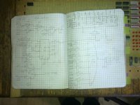
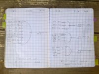
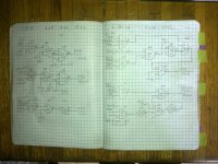
They are in two different Notebooks, And I know that there are differences between the two.. One of them is more up to date than the other.. Also, when putting them into the notebook, they are the Gate Representation of that particular chip..

001.jpg 002.jpg 003.jpg

"" 2. Checkout the registers / big mix and ALU separately.

FIG LD1 on PDF page 7 of "LD8-LD23 Schematics".pdf shows the register layout, the large MUX gate and the ALU. This is the 'heart' of the machine. I would remove all of the peripheral chips - just leaving these in place. You should then be able to bring out the 'inputs' to the remaining chips and test out the various paths with a simple 1 Hz clock and some switches. Have you done this already? ""
Awhile Back I had All of this working, then suddenly things went Bad.. But, before this I was able to do this type of thing.. I didn't do it though to the level that You are suggesting..
Also, I had put Everything into the Notebook's, WireList's, Schematics, flow diagrams, etc..

"" As the memory is connected between MA/MB and MUX(6) you should also be able to exercise the memory as well. ""

I was able to do this..

"" Only when this works in 'single-step' mode should you move on. "" Yes..

"" Document the results from each step. ""
This time I will work on doing this..
"" In fact, identify what the expected response is first (before you try the test) and ensure you get what you expect. If you don't - go back to the IC data sheets and check that you have understood what should happen. When I tried this step on my simulation of the LD30 I realised I had misunderstood how the ALU works with CIN. I had the operation inverted in my mind!

You should then be able to try something like "take AC, use the ALU to add 1 to it and store the result back in AC". You should then be able to increase the clock speed to the AC register and see what happens. It obviously should count in binary. If it starts to "stutter" as you increase the clock - you may have some noise-indices problems somewhere (or floating inputs to ICs). You may need to wire up some drivers and LEDs to see the pattern on the output from the MUX and ALU. You may have to video the LEDs if you don't have a scope or a logic analyser and play it back at slow speed to ensure that the counting is working properly. If the ALU will add 1 to the 'A' input (i.e. the output from the multiplexer) you should be able to try this test with all of the registers. I haven't got the ALU data sheet handy at the moment. ""

I had done this type of thing, before it completely went Bad..

"" I don't know how much of this you have already done - so I may be covering 'old ground' for you? ""
No, problem..
I still don'r know what it's problems were, since I had it mostly running, but it was having trouble with some instructions, and Not only do I Not know "why", but didn't have a clue as to what or how to fix these problems.. In other words I don't know How these instructions were implemented..
But, Now that the Board has been Stripped down and I am starting all over, see picture a few postings above.. Hopefully, I can work my way through it as You suggest..

THANK YOU Marty
 
Last edited:
Marty,

I'm pretty sure when you started this project you had no idea it would be this frustrating. I'm reminded of someone supposedly asking Edison if he had any thoughts on his 999 failures before getting an incandescent bulb that worked. He replied that on the contrary, from each try he learned another way not to build an incandescent bulb. It reminded be of a passage in Heinlein's "Stranger in a Strange land" where Mike, a human raised by martians is asked by his host something like this:

Jubal: "Mike, did you learn anything today?"

Mike: "Yes, Jubal. Today I learned there are two ways to tie your shoes. One is good for walking. The other is good for falling down."

Every time you tear your prototype apart and make changes to it you're learning something. Every time you post your latest "adventure" here those of us who are following it learn something as well. Eventually someone is going to get one of these working and we will all learn something.

Thank you, Marty! ;-)

DDS
 
Hi All;

DDS, Thank You for Your suggestions.. I think You responded while I was typing..

"" "Document the results from each step. In fact, identify what the expected response is first (before you try the test) and ensure you get what you expect. If you don't - go back to the IC data sheets and check that you have understood what should happen." ""

"" I'm in agreement with Dave's suggestions in general and in particular with the bit quoted above. The material posted appears to be notes from someone who was building an LD12 perhaps from a kit since there are references to inspecting parts received while they were being unpacked. "

DDS, These according to my Understanding were Part of a Course on Digital Electronics, so as each student Bought one and used it, as He/She went through the Book/Course..
And, so what we have is one of the students, Notes, Schematics and etc.., from His working unit.. See pictures in download of Ld12 of His built unit..

"" Anyone who did any kits from Heathkit or Dynaco is familiar with the process. OTOH anyone who tried to assemble the first Altair's or IMSAI's can tell you they were both nosebleeds to get debugged and running. My IMSAI User Manual is not without corrections and addenda. Take a look at many DEC boards and note that all those cut traces and added surface wire are engineering rework to correct design bugs. You may find yourself fixing errors in the original design before your LD12 actually runs reliably. When I said "boldy go where no one has gone gone before" I was only half kidding. But it's the kind of debugging that needs to be done before anyone commits to having a run of circuit boards made IMHO. "" ""
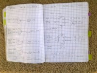
I mostly agree, Even though I have never said anything about making a Circuit Board, to me this is a wire-wrap thing only..

THANK YOU Marty
 
".... Even though I have never said anything about making a Circuit Board, to me this is a wire-wrap thing only.."

Yep. But if you go back to when people were talking about which edition of the book said what, a couple of mentions were made of getting a design working and then getting boards built so others could follow along but on an easier path. In my 42 year career as a "telephone man" I had more than my fill of wrapping and unwrapping 30 gauge wire, but soldering sockets and stuff into a circuit board? That I would do!
 
Hi All;

DDS, What did You do as a Telephone Man ??
I have a very small collection of Telephones, and an Answering Service SwitchBoard, that IS in use, as a SwitchBoard, and I have a Demo Step by Step system that is also not functioning..

THANK YOU Marty
 
Marty,

I am a bit confused about where the "notebook" in the picture came from. Is this something you created? If so, from what?

The wire lists I am referring to are "Wirelist EXT - sorted.pdf" and "Wirelist INT sorted.pdf".

These seem to be "computer generated" in some way and I can't see anything in them that states or implies that one is more up to date than the other?

These wire lists 'should' agree with the schematics from N8VEM-SBC.PBWORKS.COM I downloaded (although some of the schematics I have looked at seem to be 'partially drawn').

You need to 'divide and conquer' when it comes to this beast. The first is to get the registers, data MUX, ALU and LINK register and MEMORY up and working and thoroughly tested. Any problems here will drive you 'up the wrong path' (i.e. don't scrimp on the testing at this stage - it will only appear when you start to add the control logic).

I see you have had a lot of problems with faulty IC's. Either you are buying from a 'suspect' source or you are killing them in some way. With TTL this is usually a case of wiring an output directly to VCC by accident. Also (if you are using 74XX chips rather than 74LSXX chips) do NOT wire any input directly to the VCC rail (only do this via a pull-up resistor). I see in your 'notebook' that pull-ups to VCC have not been used for 74XX logic. Multi-input emitter transistors (used in 74XX chips) have a lower tolerance to VCC transient spikes than the power pins do and can easily be damaged. Make sure you use plenty of de-coupling capacitors (0.1 uF ceramics) and make doubly sure that your power rail is as close to +5 Volts as it can be (at the power pins of each IC). Use your voltmeter to measure at the GND and VCC pins of each chip. If you connect your voltmeter to the Power Supply ground you may not spot a volt drop in the ground wiring to the ICs.

Dave
 
Marty,

I have just had a look back at a couple of your early posts and seen a couple of lists that you have posted regarding differences between the INT and EXT net lists.

I concentrated on just one difference you highlighted (E4 pin 4) which led me to E4/A37 pin 8 (as an output) and I looked at the inputs to this gate. This is one of the many logic gates to produce PC(L) (LOADPC). In one schematic, signals A0 and F2 are used within the boolean expression - on another schematic A0 appears not to be used. One of the sets of schematics is accompanied by a boolean expression for LOADPC (which includes A0 and F2).

Question - which one do I use and which is 'correct'?

Answer - you have to work that out from first principles; as one could be equally as wrong as the other one...

I had a similar issue when I coded up my Apollo Guidance Computer (AGC) into an FPGA using the MIT schematics that I found on the internet. I spent over a year entering the schematics into EXCEL and writing some Visual Basic to validate the logic design. It was amazing what errors were thrown out by my Visual Basic. Some of them were where one schematic used the letters 'O' or 'I' or 'Z' in a symbolic name and on another schematic the symbol used the numbers '0' or '1' or '2' by mistake. These were obvious mistakes and were easily corrected. Some other warnings were identified as 'poor hardware design'. Even then, the logic still didn't work when I auto generated the VHDL for the FPGA from my EXCEL spreadsheets. In some places the schematics had indicated the use of an inverted signal when it should have indicated a non inverted signal (both of which were available). These errors took a while to track down...

Fortunately, I was doing my development in an FPGA and not hardware - but other people have shown an interest in building the AGC out of TTL. In this case I have produced what appears to be the 'correct' hardware design so that they may do what they want to do safe in the knowledge that if it doesn't work it is their implementation not the design that is at fault. If they had wired their logic up from the MIT schematics, the AGC would not have worked even if their implementation was 100% correct to the schematics because the schematics contained logic errors.

My advice is to either work out the design on paper from first principles (or at least validate what you have fully) - or invest your time simulating the logic first (either in totality or in pieces).

Dave
 
Hi All;

Dave, Thank You for Your intense answers..

""I am a bit confused about where the "notebook" in the picture came from. Is this something you created? If so, from what? ""

From the WireLists.. ""Is this something you created? "" YES !!

The wire lists I am referring to are "Wirelist EXT - sorted.pdf" and "Wirelist INT sorted.pdf".

The one You see in the Picture is from the EXT sorted wireList..

These seem to be "computer generated" in some way and I can't see anything in them that states or implies that one is more up to date than the other?

Comparing them to each other and to the Schematic, would seem that the EXT list is the better list to wire from..

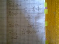
004.jpg

Dave, this picture is for Ext sorted WireList E1 and E2..
E1 is a 7430 Pin 1 goes to E1.12 with a signal name LDMA.cpo (lo) I renamed it LDMA.cpo.L..
E2 is a 7410 Pin 1 goes to the "AND" signal and goes to E1.9, E1.9 goes to L5.1 and so forth..

"" I see you have had a lot of problems with faulty IC's. Either you are buying from a 'suspect' source or you are killing them in some way. With TTL this is usually a case of wiring an output directly to VCC by accident. Also (if you are using 74XX chips rather than 74LSXX chips) do NOT wire any input directly to the VCC rail (only do this via a pull-up resistor). I see in your 'notebook' that pull-ups to VCC have not been used for 74XX logic. Multi-input emitter transistors (used in 74XX chips) have a lower tolerance to VCC transient spikes than the power pins do and can easily be damaged. Make sure you use plenty of de-coupling capacitors (0.1 uF ceramics) and make doubly sure that your power rail is as close to +5 Volts as it can be (at the power pins of each IC). Use your voltmeter to measure at the GND and VCC pins of each chip. If you connect your voltmeter to the Power Supply ground you may not spot a volt drop in the ground wiring to the ICs. ""

The decoupling Caps are one of the reasons I an redoing this whole Board, The 74xx TTL are one that I have gathered over the Years, the 74LSxx are one that I just bought, just in case, but they may not totally work because of loading differences and delay differences from the TTL that this was designed for..

"" These seem to be "computer generated" in some way and I can't see anything in them that states or implies that one is more up to date than the other?

They were compared page by page, and with the Schematics..

"" I concentrated on just one difference you highlighted (E4 pin 4) which led me to E4/A37 pin 8 (as an output) and I looked at the inputs to this gate. This is one of the many logic gates to produce PC(L) (LOADPC). In one schematic, signals A0 and F2 are used within the boolean expression - on another schematic A0 appears not to be used. One of the sets of schematics is accompanied by a boolean expression for LOADPC (which includes A0 and F2).

Question - which one do I use and which is 'correct'?

Answer - you have to work that out from first principles; as one could be equally as wrong as the other one...

I had to try them out and see if having A0 made any difference or not..

"" you have to work that out from first principles; ""

At this point I still don't know if A0 is needed or not.. But, at least in this case, it looks like A0 is not needed/used.. But, since I didn't have the Board fully functionally working, it might be needed for something I don't know about, as of yet.. Which is part of my Confusion..

"" My advice is to either work out the design on paper from first principles (or at least validate what you have fully) - or invest your time simulating the logic first (either in totality or in pieces). ""
What I am trying to say is that I am not sure that I know enough to work everything out on Paper.. I just don't have the training, nor an Engineering degree.. I would Like to though..

THANK YOU Marty
 
Last edited:
Hi All;

DDS, Thank You for the Encouragement..

Every time you tear your prototype apart and make changes to it you're learning something. Every time you post your latest "adventure" here those of us who are following it learn something as well. Eventually someone is going to get one of these working and we will all learn something.

THANK YOU Marty
 
"I just don't have the training, nor an Engineering degree.."

Not necessary. I've known graduate engineers who "couldn't find a cross in a Catholic Church" as we technicians used to say. I know, I know. Catholic churches don't have crosses. They have crucifixes. Still made a nice saying.

Drag out your breadboard and the spec sheet on your ALU. Rig up some switches on the inputs, some LED's on the outputs, some pull-ups where needed, and push a button to toggle the "clock" lead. Do the LED's on the outputs do what you expected? If so, great! If not, dig into it and find out to your own satisfaction why not. Rinse, expand, repeat and maybe ask the experts here. Like the caller on the Limbaugh show said, "It ain't rocket surgery!" Or, as my telephone instructors used to say, "Relax, its all battery and ground! It's all bits on the buss! It's all in the book! Now go back and fix it!" .When you slow everything down to the duty cycle you can achieve with your finger on a (debounced) push button great mysteries will unfold. ;-)
 
Hi All;

DDS, Thank You for the reply..
"" When you slow everything down to the duty cycle you can achieve with your finger on a (debounced) push button great mysteries will unfold. ""
I had a single step on the system before, One of the things that I had added to the system..
I can rig up the ALU and the Mux circuits, and Work through them.. I could never figure out, how the Muxes were made to work from the switches, So I still need to figure out the Logic for the different settings, then it will all probably be clear as mud to me..
THANK YOU Marty
 
Hi All;

DDS, What did You do as a Telephone Man ??
I have a very small collection of Telephones, and an Answering Service SwitchBoard, that IS in use, as a SwitchBoard, and I have a Demo Step by Step system that is also not functioning..

THANK YOU Marty

Me: Type in large paragraph detailing 42 years with "a large public futility". Submit reply.

Blog: You must be logged in to do that.

Me: Log in. Again! Retype large paragraph detailing 42 years with a "large public futility". Submit reply.

Blog: Your post is too short. Please make sure it is at least 5 characters long.

Me: Recover part of long paragraph detailing 42 years with a large public futility. Retype the rest. Submit reply.

Blog: You must log in first.

Me: Log in again. Attempt to resubmit recovered paragraph.

Blog: You have logged in since that page was updated. Please log in again and refresh.

Me. AAARRRRGGGGHHHHH!
 
I have managed this evening to start looking through the various manuals and schematics and contrasting them to each other.

I started by looking at the "A0" problem as to why it was missing from one set of schematics and not another.

The "Lab Manual.pdf" file is a very important document and (from my quick read) contains most of the information regarding how the 'computer' is 'supposed' to work. This includes most (if not all) of the key signals required to drive the registers/MUX and ALU.

Interestingly (on page 86 of the Lab Manual) the whole section on A0: seems to have had a line and a question mark scribbled by it - indicating that the section was confusing to the reader at one time or another. A little later on (page 95 to be precise), A0 is introduced into the boolean expression for MUXPC. Just prior to that, the reader has circled A0 and scribbled "what?". This may account for why figure LD14 of "LD8 - LD23 Schematics.pdf" (PDF page 5 of 17) gate E4/A37 input pin 4 is connected to F2 on pin 5 and "LD12 Schematic.pdf" page 11 of 17 has the same pin connected to A0.

A0 is used when an external interrupt is generated (from say the TTY interface) and the interrupt enable flip-flop is SET. The external interrupt starts a chain of events - which may not be processed correctly if A0 is missing from the gate above (the PC will not be loaded with whatever value is to be fed to it). As I understand the text on page 86 of the Lab Manual it says "Response to an interrupt is the execution of a JMS to location 0. ... The net effect will be to store the updated PC in location 0 followed by a JMP to location 1." I think the key phrase here is "the updated PC". When is the PC updated to point to the next instruction after the one that is being executed?

As has been said before - there is a Lab Manual and two attempts by someone to get a working system - all of which may contain different errors of one form or another.

This is a challenging project but not impossible. I think if you work your way through the book and the Lab Manual you should be able to deduce the logic for yourself independently of the schematics and then compare your work to what is in the schematics themselves.

I will print the lab manual and schematics out at work tomorrow and see what I can glean over the next few weeks. I may start to code up some of the logic in Logisim. I think I can use the bulk of the work I have already done with my LD30 implementation for the registers/MUX and ALU so it shouldn't be that onerous (we'll see if that is true or not shortly).

Dave
 
Hi All;

Dave, Thank You for the very informative paragraphs..

"" Interestingly (on page 86 of the Lab Manual) the whole section on A0: seems to have had a line and a question mark scribbled by it - indicating that the section was confusing to the reader at one time or another. A little later on (page 95 to be precise), A0 is introduced into the boolean expression for MUXPC. Just prior to that, the reader has circled A0 and scribbled "what?". This may account for why figure LD14 of "LD8 - LD23 Schematics.pdf" (PDF page 5 of 17) gate E4/A37 input pin 4 is connected to F2 on pin 5 and "LD12 Schematic.pdf" page 11 of 17 has the same pin connected to A0.

A0 is used when an external interrupt is generated (from say the TTY interface) and the interrupt enable flip-flop is SET. The external interrupt starts a chain of events - which may not be processed correctly if A0 is missing from the gate above (the PC will not be loaded with whatever value is to be fed to it). As I understand the text on page 86 of the Lab Manual it says "Response to an interrupt is the execution of a JMS to location 0. ... The net effect will be to store the updated PC in location 0 followed by a JMP to location 1." I think the key phrase here is "the updated PC". When is the PC updated to point to the next instruction after the one that is being executed? ""
This helps Explain alot about A0.. Thank You..

"" As has been said before - there is a Lab Manual and two attempts by someone to get a working system - all of which may contain different errors of one form or another. ""
I had Read and copied most of the Manual, but, it didn't make sense to me.. So, I don't fully understand A0 thru A9 and F0 thru F10 and their function, and what is used for what and where and why..

Also, Remember, that the Author May have put in the I/O and the Memory upgrade, AFTER he had or got the basic unit working..

THANK YOU Marty
 
Last edited:
"I had Read and copied most of the Manual, but, it didn't make sense to me.. So, I don't fully understand A0 thru A9 and F0 thru F10 and their function, and what is used for what and where and why.."

I don't have either edition of the book on the LD20 and LD30 and have not spent enough time looking at the documentation you posted on the LD12, but I'd like to point out that designers often give meaningful names to components of the design even if they look like gibberish to others. For Example, #1ESS/#1AESS peripheral scanners often have a lead involved with the enable/enable verify sequence called "WRMI" (pronounced wormy) that stands for "We Really Mean It." And in the #1AESS Tape Unit Controller (TUC) schematic, the gate names of the input buffer shown in a long line across the bottom of one sheet spell out "THE TUC NEEDS ALL THE HELP IT CAN GET". So I'm wondering if the names A0 through A9 and F0 through F10 have any description of their names or functions in the two editions of the book.
 
Hi All;

DDS, Thank You for the information..
"" I don't have either edition of the book on the LD20 and LD30 and have not spent enough time looking at the documentation you posted on the LD12, ""
Actually, what is in either Book is Quite different than what is in the Manual for THIS Design..
You need to use this Manual for the Descriptions of these signals, though it might be somewhat incomplete..

"" but I'd like to point out that designers often give meaningful names to components of the design even if they look like gibberish to others. ""
Actually, they were pretty good at giving names to the different signals..

"" For Example, #1ESS/#1AESS peripheral scanners often have a lead involved with the enable/enable verify sequence called "WRMI" (pronounced wormy) that stands for "We Really Mean It." And in the #1AESS Tape Unit Controller (TUC) schematic, the gate names of the input buffer shown in a long line across the bottom of one sheet spell out "THE TUC NEEDS ALL THE HELP IT CAN GET". ""
I would like to know more about the #1ESS.. Do You know anything about Step by Step Systems ??

"" So I'm wondering if the names A0 through A9 and F0 through F10 have any description of their names or functions in the two editions of the book. Not Really.. But, there is a Description in the Manual that is with these files..
They do have an F-series and and E-series in the books, which You could read and compare with what is here..

I could use an Explanation from Daver2 on A1 thru A9 and on F0 thru F10, to clarify things some..

I have re-drawn the LD-8 thru LD-14, I have LD-15 thru LD-21 to go, in my next notebook..

THANK YOU Marty
 
Hi All;

I have a question, about a sequence of gates in the accompanying pictures..

Nand Gate (G2 ) pins 4, 5 and 6 connects to Nand gate (G2 ) pins 9, 10 and 8 and this connects to Nand gate (K5 ) pins 12, 13 and 11..

Can I connect these to a 7420 4 input Nand gate with signal DCA Inverted, So that instead of having three Nand gates, I have one Nand gate ??

001.jpg 002.jpg

THANK YOU Marty
 
I have been comparing various sources of the list of ICs tonight and most of the sources agree - but one thing that jumps out to me is that there are more logic chips on the photograph of the wire-wrapped board than are in the kit.

One possibility that could account for the difference is that the board in the photograph has the memory expanded to a full 4K. I have been ignoring the memory devices themselves - but I am wondering if there are any additional 74XX series logic accompanying the memory expansion. I will check this out later.

I have also been identifying 'issues' on the schematic diagrams (e.g. unconnected input pins such as clocks, /preset, J and K inputs etc.). When I have checked the wiring lists though - they are correctly connected. The outcome is that if you are following the schematics for wiring then you will be mislead (i.e. some critical inputs will be left floating - and hence little antennas for picking up noise). If you are following the wiring lists themselves - you should be OK.

Yes, the F and A logic is the heart of the "fetch sequencer" and understanding of this is paramount to knowing how an instruction is fetched and processed before being executed. It is this logic that is responsible for detecting an interrupt, fetching the opcode from memory to the IR, incrementing the PC, handling INDIRECT operands and the like - or rather generating the sequence for such processing. I will write up a description of it later when I am not too tired (it is pretty late in the UK now).

I won't answer your NAND gate query above at this late hour - I will only screw up the Karnaugh Map!

Dave
 
Just read a bit more of post #117.

The F and E in the book stands for Fetch and Execute. The numbers after them just refer to specific Fetch and Execute States.

These should not be confused with the F and A states in the LD12 - these are all for the Fetch state!

Let me put together a more considered description of the LD12's Fetch sequencer.

Dave
 
Back
Top