• Please review our updated Terms and Rules here

Build your own PDP 8I, Part 2..

Hi All;

Daver, Thank You for Your Response, and answers..

"" I have been comparing various sources of the list of ICs tonight and most of the sources agree - but one thing that jumps out to me is that there are more logic chips on the photograph of the wire-wrapped board than are in the kit.

One possibility that could account for the difference is that the board in the photograph has the memory expanded to a full 4K. I have been ignoring the memory devices themselves - but I am wondering if there are any additional 74XX series logic accompanying the memory expansion. I will check this out later. ""

Yes, the Extra Ic's are for Both the Memory and the I/O Serial Port..
It uses 48 each 2102's just for the memory, along with other support Ic's, and another bunch for the I/O..

"" I have also been identifying 'issues' on the schematic diagrams (e.g. unconnected input pins such as clocks, /preset, J and K inputs etc.). When I have checked the wiring lists though - they are correctly connected. The outcome is that if you are following the schematics for wiring then you will be mislead (i.e. some critical inputs will be left floating - and hence little antennas for picking up noise). If you are following the wiring lists themselves - you should be OK. ""

I wired from the ExtSorted List, and not the Schematic..
There are things that are Not in the Schematic, that are in the WireList.. Like all of the Muxes, what is in the Schematic, is only a Partial Schematic of the Mux circuitry, along with the Registers..

"" handling INDIRECT operands and the like - or rather generating the sequence for such processing. ""
That is what I need the most at the present..

"" I will write up a description of it later when I am not too tired (it is pretty late in the UK now). "" That's fine..
"" I won't answer your NAND gate query above at this late hour - I will only screw up the Karnaugh Map! "" That's fine..

THANK YOU Marty
 
Last edited:
The attached PDF file I produced from an Excel spreadsheet identifies that your proposed 4-input NAND gate substitution will not give the same result as the three separate 2-input NAND gates.

I have identified the two inputs to G2 pins 4 and 5 as A and B and the output from pin 6 as Q1 respectively.

The output from G2 pin 8 as Q2.

And the output from K5 pin 11 as Q3.

I also computed the output from your transformation as "BIG NAND".

It can be seen that the columns headed Q3 and "BIG NAND" are not identical - hence your proposed transformation will not work.

For example, I used the Excel expression "=NOT( AND(A2,B2))" in the individual cells to calculate Q1.

You can use the Excel method as a quick and dirty test for any boolean expression.

When more than one FALSE started to come out of the calculation of Q3 - this indicated that a simple gate was not sufficient support the simplified logic. A NAND gate will only produce a single FALSE output when all of its inputs are TRUE (or some of them false if you use a NOT gate between them as your proposal with DCA). A single FALSE output from a simple NAND gate can, therefore, never replicate a logic system with more than one FALSE output.

I knew about the 2102 SRAM chips themselves - but good thinking about the logic to control the extra RAM chips and the serial interface.

Dave
 

Attachments

  • NAND Gates.pdf
    23.1 KB · Views: 1
Last edited:
Hi All;

Dave, Thank You for the file, and the information.. I was hoping to eliminate some gates..

I have almost copied most of the New Schematics and then I will need to assign gate numbers and pin assignments..
And see if there are a few less Ic's and a more smoother timing situation..

THANK YOU Marty
 
Hi All;

Dave, Thank You for the compliment ..

"" I give you 10 out of 10 for your notebook - very neat and tidy! ""
I don't know of any other way, to keep everything together and in a somewhat organized manner..
Where any changes are easy to make, and figure out..

I have added Timing delays to some of Fxx and Axx signals, where needed, so that the signals come in at the same time, as the rest of the circuit.. Not Elegant, but it should serve the purpose..

For present, I think I have it all drawn out.. I need to put in Gate numbers and pin numbers next..
I am also making a WireList for this unit, with signal names..

THANK YOU Marty
 
Last edited:
I got some slack time today and (mis)used some of it to slog through parts of the Lab Manual. All I can say is it's clear as mud in some places. Even when I was pretty sure I knew what he was trying to say I was still shaking my head at the end of his explanation. I would have been one very unhappy camper if i was in his class and the Lab Manual was all I had to go on. I'm going to bet there was a lot of additional explanation going on in the lecture sessions. Just one small example. A 74xx00 is not an AND gate. It's a NAND gate. And it's called a NAND gate in the Texas Instruments catalog that the instructor refers to. There's also a tricky part about the clock design and whether or not the clock should be "gated" that you might want to look at. He mentions that the design could be more fault tolerant if a chip that wasn't then readily available were used. He also mentions the use of a 74Lxx chip in one spot because they're less likely to trigger on spikes. When you mentioned earlier that you were getting different results on different test runs I started thinking "unstable clock". Might be a good place to look.
 
Hi All;

DDS, Thank You for the Response..
"" A 74xx00 is not an AND gate. It's a NAND gate. And it's called a NAND gate in the Texas Instruments catalog that the instructor refers to. ""
I think that this is a Typo..
"" I'm going to bet there was a lot of additional explanation going on in the lecture sessions. ""
Yes, I wish I had a Recording of those lectures..
"" There's also a tricky part about the clock design and whether or not the clock should be "gated" that you might want to look at. He mentions that the design could be more fault tolerant if a chip that wasn't then readily available were used. ""
He used a 555 for the clock chip and buffered it with numerous NAND and NOT gates..
"" He also mentions the use of a 74Lxx chip in one spot because they're less likely to trigger on spikes. ""
Also the 74L00 was used as it has the longest Delay Time, for Lengthening the flip-flop pulse..
"" When you mentioned earlier that you were getting different results on different test runs I started thinking "unstable clock". Might be a good place to look. ""
As mentioned Earlier, I used a very slow clock pulse, But my pulse was half cycle, same time up as time down.. Which also might have been some of the problem, Instead of like ten to one.. One time up and nine times down for settling..

THANK YOU Marty
 
Last edited:
"A 74xx00 is not an AND gate. It's a NAND gate. And it's called a NAND gate in the Texas Instruments catalog that the instructor refers to." I think that this is a Typo..

Well, not really...

The Lab manual on page 15 identifies a 7400 as an "AND" gate (even though it is a NAND gate) and also a 7402 as an AND gate (even though it is a NOR gate). Then look down to page 31 of the Lab manual and you will see that a 7400 is described as an OR gate! What's going on?

It depends upon whether you are drawing (what I will call) a "physical" schematic or a "logical" schematic. If you were drawing a physical schematic you would draw each gate of a 7400 as a NAND gate - end of story. If you were drawing a logical schematic you could draw a 7400 gate as either a NAND gate or as an OR gate with inverted inputs.

Check out the first schematic of "LD8 - LD23 Schematics.pdf" in the upper right hand corner (if printed the right way around in landscape that is). You will see a 7430 (E15/A21) which is an 8-input NAND gate drawn as an OR gate with inverted inputs. Look back a bit to G4/A49 (a 7400) - this is a NAND gate package drawn as an OR gate with inverted inputs. Even more bizarre is K8/A28 and K7/A25 (both 7402 NOR packages). One is drawn as a NOR gate 'properly' with the other drawn as an AND gate with inverted inputs.

This indicates that the schematics are drawn logically rather than physically - so you need to beware of this when reading them.

Just in case you are confused at this point, DeMorgan's states that a NAND gate can be replaced by an OR gate with inverted inputs and a NOR gate can also be replaced by an AND gate with inverted inputs. (i.e. you can physically create a NOR gate with an AND gate and some inverters - or you can draw a NOR gate as an AND gate with inverted inputs).

You must also remember that this is a Lab associated with a University Course - so some of the material may not follow what you expect from (say) an electronics constructional project. Whilst reading the book that Marty recommended, I came across a line symbol on some wires that I did not understand. I had to go back to earlier chapters of the book to understand what this particular symbol actually meant in the context of the course. I have also seen this same symbol numerous times on the Lab schematics - so understanding why it is there is important.

Sorry - work is getting in the way of answering your Fx/Ax query. I will get around to it shortly - I promise.

Dave
 
Hi All;

Dave, Thanks for the explanation..
I don't know if You have either book, But, He is trying to show/teach mixed logic, that way His students would get used to seeing either symbol for a the type of logic that is being used to convey, what is happening..
So, I think either book most likely do a better job of conveying this, or maybe after writing this numerous times the explanation just got better..

"" Sorry - work is getting in the way of answering your Fx/Ax query. I will get around to it shortly - I promise. ""

I didn't know I had a query.. I was just stating what I was doing..
Such as, in LD-13, ALU Signals, the schematic for the Cin.. Shows the signals to M10 (7430), that they arrive at the 7430 at different times, so what I am trying to do is make them all, closer in time together..
On the 7430 pin 1,2 You have a four gate delay, on pin 3, it is the same thing, pin 4 and pin 5 have a one gate delay..
And for the A0, F2 and F7 a No gate delay.. So I redid the circuit, so that they all have a two gate delay and so all the signals arrive at the 7430 at the same time.. And the Output of the 7430 goes to another gate, thereby the total is a three gate delay, which is the same as what is used for the S0, S1, S2, S3 and M signals as well.. That way all of these signals arrive at the same time to the ALU..

THANK YOU Marty
 
Yes, I have the second edition of the book.

I was trying to answer DDS about why the Lab notes talk about a 7400 as an AND gate in some places.

Yes, you really need to read the Lab notes in conjunction with the book (since the lecture notes are not available to us and the book was - I think - recommended reading for the course).

Back in post #117 you were asking "I could use an Explanation from Daver2 on A1 thru A9 and on F0 thru F10, to clarify things some..". This was what I was meaning to do. Do you now understand what the Fx and Ax signals do (hence I don't need to provide the explanation any more)?

I don't see why you are going to all the trouble of equalising the gate delays to such things as the ALU? From the register outputs through the MUX and the ALU back to the registers is a combinatorial path (i.e. devoid of clock signals). All that matters is that the data arriving back at the registers is stable just before the clock latches the data back into the registers. It may help if noise is present - but that is more by luck than design.

Just as a matter of interest - are you using Fairchild 9024 JK flip-flops in your implementation or have you replaced these with an alternative?

Dave
 
Hi All;

Dave Thank You for the Explanation..
"" I was trying to answer DDS about why the Lab notes talk about a 7400 as an AND gate in some places. ""
OK, that explains it..
"" Back in post #117 you were asking "I could use an Explanation from Daver2 on A1 thru A9 and on F0 thru F10, to clarify things some..". This was what I was meaning to do. Do you now understand what the Fx and Ax signals do (hence I don't need to provide the explanation any more)? ""
YES, Please !! Maybe Your explanation, will help me understand about Your answer on the next paragraph..
"" I don't see why you are going to all the trouble of equalising the gate delays to such things as the ALU? From the register outputs through the MUX and the ALU back to the registers is a combinatorial path (i.e. devoid of clock signals). All that matters is that the data arriving back at the registers is stable just before the clock latches the data back into the registers. It may help if noise is present - but that is more by luck than design.
Since, before I would get different answers, at different F states and some of the differences, would be the ALU doing one thing at (say) F0 one time and something different at F0 the next time.. So, S0-S3 and M are the same, but Cin is different, and so one time it Increments and another it Passes the contents on..
I hope that this is as clear as Mud..
"" Just as a matter of interest - are you using Fairchild 9024 JK flip-flops in your implementation or have you replaced these with an alternative? ""
A 74109..

Just for the fun of it, and to stir my clear as muded mind, I am going to Read His chapters in Both Editions on His MicroProgrammed Design..
I have looked at both descriptions, in each of the Editions of the book, and they are Both different for the most part..
Though, the Second Edition of the Book is a far better Description of Implementing the the PDP 8i using Bit Slice Ic's, there are alot of holes in its Description, that is much left up to the Reader to figure out..
It does use Forth on its MicroComputer to implement the code for the Bit Slice Processor..
So as for me it is and would be far easier to implement the PDP 8i as I am doing, than to do so in/with Bit Slice Technology, because of the added burden of writing and implementing the additional Code and Hardware to make the Bit Slice's work..
But, Yes once the Supporting code and Hardware are done, then Yes, it would be easier and far less Ic's to implement it using Bit Slice..
THANK YOU Marty
 
Last edited:
Hi All;

I found another mistake, that I had previously wired wrong.. But, I didn't know that it was wired wrong..
On the Ext wirelist, On K12 it shows pin 2 of the 7400 wired to CP5.H, pin 1 goes to IR10.H, pin 3 is therefore IR10.CP5.L and this connects to K3.12, a 7402 K3 pin 11 Halt.L (OPG2.IR10), pin 12 is IR10.CP5.L and its Output is pin 13 OPG2.IR10.CP4..
What shouldn't that be CP5, well tracing it back and looking at the schematics, the CP5 was Mislabeled and should have been CP4, all along..
BUT, Looking at the Lab Manual, under LD-3, that shows it should be CP3 !!! And Not CP4 or CP5..
I think I will need to try all three and see which one works better or more correct..

THANK YOU Marty

Look at "LD12 Schematic.pdf". On page 5 a bit left of center is a chip that counts pulses from the clock and generates the discrete CPn leads for each clock interval CP0 thru CP7. Now look at "Lab Manual.pdf" on page 104 there's a chart showing leads developed for various instructions for each CPn interval. If some of your chips were being enabled earlier or later than they should have been you may have found at least one of the reasons for the flaky results you were getting.
 
Hi All;

DDS, Thank You for Your reply..
"" Look at "LD12 Schematic.pdf". On page 5 a bit left of center is a chip that counts pulses from the clock and generates the discrete CPn leads for each clock interval CP0 thru CP7. Now look at "Lab Manual.pdf" on page 104 there's a chart showing leads developed for various instructions for each CPn interval. If some of your chips were being enabled earlier or later than they should have been you may have found at least one of the reasons for the flaky results you were getting. ""
That is exactly where I was looking at ( Lab Manual page 104) .. And I knew about the the 7442 that Generates the CPx signals..
What I think I will need to do is make another chart that Traces the Wire Listing for each of the CP Signals and compare them to what is on Page 104 of the Lab Manual, and if or what other CP mistakes there might be.. Also, it would be a good Idea to check the rest of the chart against what was wired..
"" If some of your chips were being enabled earlier or later than they should have been you may have found at least one of the reasons for the flaky results you were getting. ""
Yes, that would explain alot of what I was seeing, and not knowing where to look.. So, while I am re-doing my Notebook and wire lists, I can check for other misprint mistakes.. And make some more flow charts..

THANK YOU Marty
 
Hi All;

I just got some wire, so now I don't need to use just little pieces of wire, and try to find something long enough..

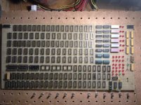
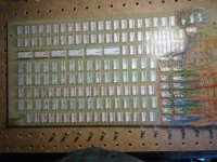
Here is a picture of what might be, plenty of room, I hope..

002.jpg

I am still working on Placement of the Ic's..
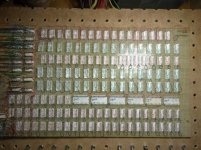
Placement is done, with some room left over, but not much.. Most rows have a couple of unassigned places..
Now to wire up Power and Ground..

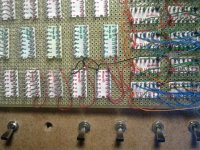
001.jpg 002.jpg

Power and Ground is going to be more difficult than before..

THANK YOU Marty
 
Last edited:
My - your construction looks mighty nice...

I have started 'in earnest' entering the schematics into Logisim. As I was doing this - I am coming across all sorts of discrepancies. Some with the Lab manual descriptions of signal derivations, some with how the Lab manual signal derivations are implemented by the schematic etc. etc. etc.

I am doing the 'simple logic' for now (e.g. the registers and the bulk of the combinatorial logic dealing with the MUX and ALU control signals, decoding of the OPR instruction (group 1 and 2) and register loading).

I was horrified by the logic for the register loading signals [e.g. MB(L)]. You need to be VERY careful with the type of gate in the /CLEAR side to prevent you getting a very short 'runt pulse' that will not be seen by the registers (or may be seen only under certain circumstances). Are you actually using a 74L00 in this position?

I agree with DDS - that some of this 'design' looks (and probably behaves) strange...

I will post my logisim design when I have completed it, ironed out the bugs and it runs some of the diagnostics.

PS: You don't need a bit slice processor for a microprogrammed design. My LD30 logisim implementation just uses a 7-bit loadable binary counter, some fast ROM and a couple of multiplexers and D-type latches.

Dave
 
Hi All;

Dave, Thank You for Your Answer, and willingness to enter this in..
"" I was horrified by the logic for the register loading signals [e.g. MB(L)]. You need to be VERY careful with the type of gate in the /CLEAR side to prevent you getting a very short 'runt pulse' that will not be seen by the registers (or may be seen only under certain circumstances). Are you actually using a 74L00 in this position? ""
YES, I have a few 74Lxx Ic's, even though with You mentioning it, I think I will put in a 7408, followed by a 74L00, Used as an inverter to lengthen it a bit more.. I will need to see what I have, to implement this /Clear signal..

"" I agree with DDS - that some of this 'design' looks (and probably behaves) strange... ""
Any Ironing out You can do, Please let me know about..

""I will post my logisim design when I have completed it, ironed out the bugs and it runs some of the diagnostics. ""
Please post it,before you have Ironed out the Bugs, and I (at least) can see the progression and possibly the "why" of what You are doing or did..

THANK YOU Marty
 
Last edited:
A couple of ideas:

1. In looking at the parts list in the Assembly manual I noted that of the IC's listed, every one was a plain vanilla 74nn except for one lonely 74Lnn. Nowadays anything that's being created using TTL pretty much defaults to the 74LSnn series. The internet was being difficult about when the 74LSnn series was released. My TI TTL Data Book is second edition copyright 1976 and the 74LSnn parts are in it. What dates I see in the LD12 materials are in 1974. Perhaps the short note in the Lab Manual about devices not yet readily available refers to the 74LSnn family?

2. Speaking of dates in the LD12 materials, many of the schematics have dates on them. Some like LD12 Schematic.pdf page 5 have many. To me they're suggestive of revision dates. That bothers me because they suggest that bugs were found and fixed and the drawings updated, but nothing tells us what was changed or why. It would be helpful if any bugs or typo's found are documented here or on the nv8em website with the rest of the documents. Any useful information like lead names, IC types and location and pin numbers should be clear enough so that someone else 10 years from now doesn't have to debug this stuff all over again.

3. There are some notations on the schematics I find puzzling. Referring again to the LD12 Schematic.pdf page 5 lower left corner is a gate, apparently on a 7430 that's also labeled A10. Are these IC's numbered in a coordinate fashion like row and column? If so I'm guessing the A10 inside the gate symbol is the location on the original design. If that's correct, what does the M16 just above the gate refer to?

4. I'm also going to start tinkering around for the first time with Logisim. And I would appreciate it if any corrections you guys find that we and future tinkerers might need be documented here and/or on the nv8em site as well.
 
Hi All;

Thank You, DDS for Your suggestions..

"" 1. In looking at the parts list in the Assembly manual I noted that of the IC's listed, every one was a plain vanilla 74nn except for one lonely 74Lnn. Nowadays anything that's being created using TTL pretty much defaults to the 74LSnn series. The internet was being difficult about when the 74LSnn series was released. My TI TTL Data Book is second edition copyright 1976 and the 74LSnn parts are in it. What dates I see in the LD12 materials are in 1974. Perhaps the short note in the Lab Manual about devices not yet readily available refers to the 74LSnn family? ""
I have Plenty of the plain 74xx, so for now until I can get it working, and then try the LS.. At present it is not a speed thing, But, more than likely a TTL Load thing..

"" 2. Speaking of dates in the LD12 materials, many of the schematics have dates on them. Some like LD12 Schematic.pdf page 5 have many. To me they're suggestive of revision dates. That bothers me because they suggest that bugs were found and fixed and the drawings updated, but nothing tells us what was changed or why. It would be helpful if any bugs or typo's found are documented here or on the nv8em website with the rest of the documents. Any useful information like lead names, IC types and location and pin numbers should be clear enough so that someone else 10 years from now doesn't have to debug this stuff all over again. ""
I don't remember for sure, whether I have put all that I found here, or not.. I think I did..

"" 3. There are some notations on the schematics I find puzzling. Referring again to the LD12 Schematic.pdf page 5 lower left corner is a gate, apparently on a 7430 that's also labeled A10. Are these IC's numbered in a coordinate fashion like row and column? If so I'm guessing the A10 inside the gate symbol is the location on the original design. If that's correct, what does the M16 just above the gate refer to? ""
The M16 is the IC designation from the Externally Sorted List, and the A10 Refers to the Internally Sorted List..

"" 4. I'm also going to start tinkering around for the first time with Logisim. And I would appreciate it if any corrections you guys find that we and future tinkerers might need be documented here and/or on the nv8em site as well. ""
I think we can put updates here.. I don't know how to add them to the nv8em site..

THANK YOU Marty
 
Back
Top