| VCF West | Aug 01 - 02 2025, | CHM, Mountain View, CA |
| VCF Midwest | Sep 13 - 14 2025, | Schaumburg, IL |
| VCF Montreal | Jan 24 - 25, 2026, | RMC Saint Jean, Montreal, Canada |
| VCF SoCal | Feb 14 - 15, 2026, | Hotel Fera, Orange CA |
| VCF Southwest | May 29 - 31, 2026, | Westin Dallas Fort Worth Airport |
| VCF Southeast | June, 2026 | Atlanta, GA |
-
Please review our updated Terms and Rules here
You are using an out of date browser. It may not display this or other websites correctly.
You should upgrade or use an alternative browser.
You should upgrade or use an alternative browser.
C64 IN PET S' CASE
- Thread starter Desperado
- Start date
daver2
10k Member
You sure are!
I would be inclined to 'turn around' your ICs though so that VCC is at the top right and GND is at the bottom left. This is generally how ICs appear on datasheets and in schematics.
You didn't expect to be doing this when you woke up this morning did you!
Dave
I would be inclined to 'turn around' your ICs though so that VCC is at the top right and GND is at the bottom left. This is generally how ICs appear on datasheets and in schematics.
You didn't expect to be doing this when you woke up this morning did you!
Dave
Desperado
Veteran Member
- Joined
- Nov 25, 2017
- Messages
- 7,880
Ops....this means i have to redo everything from the beginningI would be inclined to 'turn around' your ICs though so that VCC is at the top right and GND is at the bottom left. This is generally how ICs appear on datasheets and in schematics.

daver2
10k Member
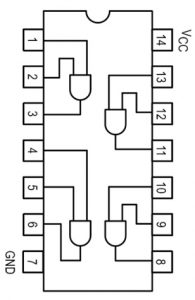
Slight correction. You have ONE 74LS08 IC not two.
The way KiCAD draws them is as individual gates. It looks like the way this tool draws them is as a complete IC package.
Look at the pin numbers on Ruud's schematic - they are the same pin numbers on your IC package.
Dave
The way KiCAD draws them is as individual gates. It looks like the way this tool draws them is as a complete IC package.
Look at the pin numbers on Ruud's schematic - they are the same pin numbers on your IC package.
Dave
daver2
10k Member
>>> Ops....this means i have to redo everything from the beginning.
No. JUST THE IC PACKAGE. Not everything else!
But read my post above.
Dave
No. JUST THE IC PACKAGE. Not everything else!
But read my post above.
Dave
daver2
10k Member
The first sign of a learning opportunity and the white flag goes up!
All you have mistaken is that there is a difference between gates and IC packages...
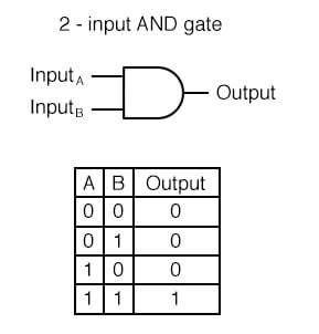
A 74LS08 package contains four gates. A 74LS123 contains two monostables.
If you look at the photograph of the PCB you will see three (3) ICs - all you have to do is to drop the correct ICs onto your schematic and wire up the pins according to Ruud's schematic.
Where it says IC1A, IC1B etc. these are individual gates in your IC1. The pin numbers are the same between Ruud's schematic and yours.
Dave
All you have mistaken is that there is a difference between gates and IC packages...
A 74LS08 package contains four gates. A 74LS123 contains two monostables.
If you look at the photograph of the PCB you will see three (3) ICs - all you have to do is to drop the correct ICs onto your schematic and wire up the pins according to Ruud's schematic.
Where it says IC1A, IC1B etc. these are individual gates in your IC1. The pin numbers are the same between Ruud's schematic and yours.
Dave
daver2
10k Member
These are GATES not IC PACKAGES.on the ruud s' schematic i see:
4 74ls08
2 74ls221
2 74ls123
There is 1 74LS08 IC PACKAGE containing 4 individual GATES.
How many physical ICs can you see on the video board in your photograph?
Dave
Desperado
Veteran Member
- Joined
- Nov 25, 2017
- Messages
- 7,880
3!These are GATES not IC PACKAGES.
There is 1 74LS08 IC PACKAGE containing 4 individual GATES.
How many physical ICs can you see on the video board in your photograph?
Dave
In case you're still confused: if your circuit needs 4 logic AND gates and a 74LS08 contains 4 AND gates, are you going to buy 4 ICs and just use 1 gate or are you going to use all 4 ")
I might be interested in having one of these boards too. I thought of designing it but it's more fun to watch you doing it... don't give up!
I might be interested in having one of these boards too. I thought of designing it but it's more fun to watch you doing it... don't give up!
Desperado
Veteran Member
- Joined
- Nov 25, 2017
- Messages
- 7,880
Ok thanks so much!In case you're still confused: if your circuit needs 4 logic AND gates and a 74LS08 contains 4 AND gates, are you going to buy 4 ICs and just use 1 gate or are you going to use all 4
I might be interested in having one of these boards too. I thought of designing it but it's more fun to watch you doing it... don't give up!
I am trying now!
daver2
10k Member
Correct!
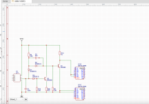
So you should only have 3 IC packages on your schematic (if this is how the schematic editor works).
You're doing well...
I was out at our Church doing some work - so I was on my phone - which is not exactly user-friendly!
Dave
daver2
10k Member
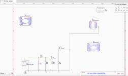
Yes, but why did you delete the rest of the analogue circuitry? There was no need for that...
Are there SN74LSxxxN packages available rather than the 'D' part that you have used. A 'D' package is surface mount not through hole. An 'N' package is through hole.
You also don't have to use lots of 'green wires' to connect everything up like you have (e.g. pins 9 and 10 of IC1 is connected to GND). You can use the GND symbol to pins 9 and 10 instead of a green wire. Likewise, you can use the VCC symbol. Don't forget to wire up the GND and VCC pins of the IC packages to GND and VCC - otherwise they haven't got any voltage! This makes your schematic less 'cluttered' with wires.
Dave
daver2
10k Member
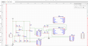
The other thing I notice is that your JP1 header is 2x4 and it should be 1x4. You already had the correct part back in post #37. You just needed to flip the symbol so the connections were to the right hand side rather than to the left hand side.
Ditto for JP2 - it should be a 1x7 header and it looks like 2x7.
Dave
Ditto for JP2 - it should be a 1x7 header and it looks like 2x7.
Dave
Desperado
Veteran Member
- Joined
- Nov 25, 2017
- Messages
- 7,880
It s very difficult job for meThe other thing I notice is that your JP1 header is 2x4 and it should be 1x4. You already had the correct part back in post #37. You just needed to flip the symbol so the connections were to the right hand side rather than to the left hand side.
Ditto for JP2 - it should be a 1x7 header and it looks like 2x7.
Dave
daver2
10k Member
It isn't - you did an excellent job of the analogue circuitry back in post #41.
You just went a little astray with the ICs in post #46.
All you had to do was to delete the extraneous ICs that you accidentally included from post #46 and carry on.
This is your first day of using a completely new software tool and learning a bit more about electronics, schematics etc.
Perhaps time to have a glass (or 2) of wine and attack it again tomorrow...
There is always a learning curve with anything new. This is how we all progress.
Dave
Yeah you'll get there. I drew my first schematic+PCB a couple of weeks ago, had a bit of delicious local beer for encouragement. The boards arrived today and work exactly as planned. I used a different EDA tool but I'd guess they're all pretty similar and once you get a routine going with the tool you use, you'll become more or less unstoppable - I've designed a couple more boards while waiting for the first to arrive. Each took less time than the previous one.