Desperado
Veteran Member
- Joined
- Nov 25, 2017
- Messages
- 6,827
i don't believe that with only the kernel can be enoughThe easiest solution would be using the 4064 kernal and stick with the mono TTL video

i don't believe that with only the kernel can be enoughThe easiest solution would be using the 4064 kernal and stick with the mono TTL video
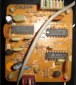
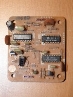
This looks really easy. In fact if you had a photo of the rear of this pcb you could reverse engineer it in a heartbeat. Even without that though, Ruud's schematic will match it, so you can simply place the components as shown on this pcb photo and make the tracks conform to the schematic.I found this picture on web.... Cbm 4064 video output:
 !
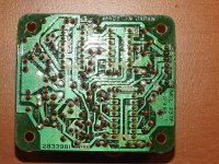
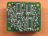
!Yes I would love to but I don't know how to proceed...Why don't you have a go at creating the PCB yourself? Learn a new skill...
Great!>>> Yes I would love to but I don't know how to proceed...
Pop over to: https://easyeda.com/. I wonder if there is an Italian language option for you?
You enter the schematic (follow Ruud's original).
Assign footprints to each component.
Move and orientate the footprints to match the solder-side photograph you have found.
Interconnect the terminals of the footprints (components) to match the copper tracks on the photograph.
OK, there is a learning curve to go up - but that is why we are here. Have a go - it is free - so it won't cost you anything financially.
The PCB is single-sided (from what I can see) so there is no hidden 'magic' to work out.
Dave
!