• Please review our updated Terms and Rules here

Cbm 2001 Pet strange boot

Yes, but you are going have to describe in the post what you were doing at the time. I don't have a crystal ball I am afraid!

Were you permanently monitoring the two (2) signals all the time - and the waveform was changing as indicated?

Dave
Ops sorry Dave!1
In the first part of this last video I was measuring the two channels, when you see channel 2 disappear, it was I who disconnected the probe!
 
So using the oscilloscope to do this appears to be beyond your current capabilities I think.

How would you feel about removing the CPU and making up some 'jumper' cables for the address bus so that we can 'force' address $F000 onto the address bus (in READ mode) and then we can examine the data bus way more easily.

Dave
Is difficult to do this? :(
 
Nope - it should just be 17 (or so) wires 'poked' into the CPU socket where the address lines are connected to either 0V or VCC.

Dave
 
From the CPU socket to the CPU socket...

Remove the CPU from it's socket.

Connect pin 34 (R/W) to VCC (pin 8) via a resistor (something like 100 Ohms).

Connect AB0 .. AB11 of the CPU socket to 0V (pin 1).

Connect AB12 .. AB15 of the CPU socket to VCC (pin 8) via another resistor (something like 100 Ohms).

This will force a read from address $F000 (with hope).

You should observe AB0 .. AB11 of the ROM UD9 to be '0'.

You should observe UD9 pin 20 as permanently '0'.

Measure the eight data lines for the UD9 ROM and report their values back.

You may as well use your logic probe for this work.

Try not to damage the IC socket that the CPU sits in - so don't use too thick a wire.

As there are a lot of wires going to be connected to 0V, you may need to make up a little 'fan out' unit so that one piece of wire is split up into multiple wires.

If you have some prototyping board - this may make life easier.

Also, be careful not to short anything out. This is why I would use some 100 Ohm (or so) resistors on the VCC rail to limit any current flow in case of problems.

Dave
Dave, I've thought about it and unfortunately I have to give up ... it's getting too complicated and I don't think I need to keep bothering you and everyone else ... With regret I have to stop .... What I will do is send the card to a friend of mine here in Italy, he has already repaired a pet card some time ago and he will surely find some simple little damage that I can't see. I thank everyone for the help you have given me so far but I don't feel like making all these jumpers on the cpu ...
 
Look, this is virtually the last thing to do. It is worth doing this to see if the data bus is giving us sense or not. But, if you are going to send it to your friend, then I would still like to see it repaired!

Dave
 
Look, this is virtually the last thing to do. It is worth doing this to see if the data bus is giving us sense or not. But, if you are going to send it to your friend, then I would still like to see it repaired!

Dave
Dave i am ready for the measures...can i use logic probe on ud9 pin 9 to 25?
 
UD9:

9: H
10: L
11: L
12: L
13: L
14: L
15: L
16: L
17: L
18: L
19: L
20: L

PIN 26 TO 33 : NO SIGNAL!!! :((((
 
>>> Dave i am ready for the measures...can i use logic probe on ud9 pin 9 to 25?

Yep!

So, this EPROM should have been erased shouldn't it? So all of the data bit outputs should be HIGH.

Pin 9 is HIGH (which is correct) - but pins 10, 11 and 13-17 should be high as well.

The data pins on the CPU (26 to 33) should follow the data pins of the EPROM. SO this is definitely wrong. There SHOULD be copper tracks between the ROM and the CPU. You did remove the NOP generator didn't you?

You need to investigate the NO SIGNAL issue - as this is fundamental (and will account for our problems).

Dave
Yes Dave, i have an empty eprom on ud9 and without cpu and nop... i am desperate!!
 
Stop being desperate and work the problem through...

With the power OFF - check for continuity from the data lines of ROM UD9 to the data lines of the CPU socket with your multimeter.

Dave
 
Desperado: I have attached a diagram to help explain what Dave has asked you to do.

It is important that you understand what is going on.

In the PET manual the schematic is broken onto different pages. So I have added the UD9 ROM onto the same page as the CPU diagram. The links in black lines I drew in, are pcb tracks, already there in the computer to be checked.

The idea, as you can see from the diagram, is to force the address $F000 onto the address bus by adding the wire links shown in Red & Blue. This should cause SelF to go low and the ROM D9 to be selected. It will receive all zero's on its address input, selecting the first memory location in it. So if this memory location holds an FF (which it should do if the ROM is blank) then all the ROM's output (Data) lines will be high. In this system of testing Dave has devised for you, there are no pulses so you can just take your time and use your meter or logic probe looking for Highs or Lows.

So what Dave has given you here is a way to test the continuity of the tracks and connections in this large loop which links the CPU and ROM UD9, and it also checks that the address buffer IC's are working too because they are in this big loop of connections.
 

Attachments

  • CPU1.jpg
    CPU1.jpg
    337.9 KB · Views: 10
Stop being desperate and work the problem through...

With the power OFF - check for continuity from the data lines of ROM UD9 to the data lines of the CPU socket with your multimeter.

Dave
Hi Dave, need i check continuity with all wires on cpu socket or not? Thanks!

@Hugo Holden thanks so much for the diagram!
 
PIN ROM TO CPU CONTINUITY:


9-33 OK

10-32 OK

11-31 OK

13-30 OK

14-29 OK

15-28 OK

16-27 OK

17-26 OK
 
Thanks.

What you are posting in #2,051 is not really possible then...

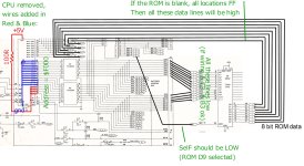
Can you use your logic probe and check the data levels on each pin of UD9 and post back the results please.

Can you also measure the DC voltage (using a digital multimeter) at the actual UD9 ROM itself (black lead to pin 12 and red lead to pin 24).

Can you also measure the DC voltage on the /CS line (using a digital multimeter) at the actual UD9 ROM itself (black lead to pin 12 and red lead to pin 20).

Then double-check (with the logic probe) the logic levels on the CPU socket pins 33, 32, 31, 30, 29, 28, 27 and 26 again.

You have checked the continuity from the CPU data bus pins to the ROM data bus pins. You haven't detailed the actual resistance though. That would be useful to know. Should be < 1 Ohm. So, there should be absolutely no reason why the logic levels on the UD9 ROM data bus are any different to those on the CPU socket. If they are - there is something strange going on. But what...

Dave
 
With a BLANK EPROM installed. We are NOT changing the configuration unless I tell you.

Remember that we don't change the configuration?

The BLANK EPROM should be producing the VOLTAGE that we should be measuring on the data bus.

Dave
 
Back
Top