• Please review our updated Terms and Rules here

Classic PDP-8 Donation at the RICM

I've had some luck with hand-spinning (wood) rods held in fine sandpaper to reduce their diameter slightly. Would that make some of the thicker rod segments useable?
Sometime I need to put a project away for a day, and try again later. Saturday I will trial fit just the Acrylic rod to make sure that it fits into the metal bracket holes before I add glue and try to install the paddle. It is also possible that I drilled the pivot hole little off center so I need to check the clearance for the switches' metal bracket on the paddle.
 
It is also possible that I drilled the pivot hole little off center so I need to check the clearance for the switches' metal bracket on the paddle.
This is possible unless you are careful when you clamp the drill guide to the base of the drill press. It is also essential that the base of the drill press be perpendicular to the bit. And that is sometimes difficult to ascertain. I considered using a friends vertical milling machine to drill the holes but it turned out I got everything lined up.

The way I line it up is to extend the bit with the drill turned off into the hole in the base of the guide. While holding the drill fully extended through the base of the guide so that the chuck touches the guide, then apply the clamps. The bit through the hole will ensure the base is centered on the bit. There is not a lot of force applied when drilling so you don't need to overtighten the clamps and deform the guide.

If you managed to drill a hole off center or at an angle you can fill it with epoxy (something like JB weld and re-drill it after a couple of days of curing.
 
If you managed to drill a hole off center or at an angle you can fill it with epoxy (something like JB weld and re-drill it after a couple of days of curing.

Or I could drill the hole a little larger, put Gorilla glue in the hole, insert the pivot pin, and assemble the switch. When the glue dries there will be enough clearance between the paddle and the switch bracket.
 
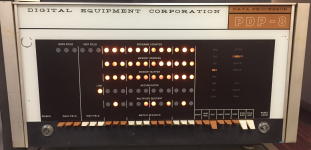
We are making progress on the recently donated DEC Classic PDP-8. All of the front panel switch paddle pivots have been repaired, thanks to Doug for the drill fixture. Fortunately all of the front panel lights are working, so I don't need to do more fiddly work there. The resistance of the bulbs varies, so I imagine that some incorrect bulbs were substituted. The next step is debug and repair. The STOP switch doesn't stop the processor. That might be an easy problem to fix first.

1722263069211.png
 
Page 10-41 in F87 maint manual. Print is labeled HS-D-8P-0-9 Timing, Keys, Switches, and Run Control. Page 274 of the PDF on Bitsavers.
Page 10-65 through 10-69 are the pinouts for some of the front panel connectors.
Page 10-77 is the pinout for one of the front panel connectors.
Page 10-78 is the pinout for one of the front panel connectors.
Page 10-89 is the pinout for one of the front panel connectors.

I know I have seen a diagram for the front panel itself, but I didn't find it on my quick search. Most of what you want is on page 10-41. That is the logic for the switches.

Maybe the front panel schematic is in my box of C size drawings. They are so fragile I don't like to mess with them unless I have to.
 
Page 10-41 in F87 maint manual. Print is labeled HS-D-8P-0-9 Timing, Keys, Switches, and Run Control. Page 274 of the PDF on Bitsavers.

I have been using this page to see what the switches do. Unfortunately the section between the switches and the R302 that makes the SP* signals has been modified in our PDP-8. Also the CLOCK input to the R202 for the TG flip-flop has also been modified. I need to reverse engineer the changes and redraw the schematic.

Page 10-65 through 10-69 are the pinouts for some of the front panel connectors.
Page 10-77 is the pinout for one of the front panel connectors.
Page 10-78 is the pinout for one of the front panel connectors.
Page 10-89 is the pinout for one of the front panel connectors.

I know I have seen a diagram for the front panel itself, but I didn't find it on my quick search. Most of what you want is on page 10-41. That is the logic for the switches.

Maybe the front panel schematic is in my box of C size drawings. They are so fragile I don't like to mess with them unless I have to.

I missed all of those expecting to find a schematic.

Thanks for the help!
 
We found a shorted D-662 diode D1 on the S107 FlipChip in slot PD31 that was causing problems with the STOP and SINGLE STEP functions.

Memory EXAM works, but DEP does not. I work on that next.

We bought some industrial Acrylic adhesive and some 1/2"x1/2"x6" pieces of Acrylic. We will use that to glue and then reinforce the corner joints in the Acrylic system covers.
 
We noticed that the MEMORY ADDRESS bit-3 is always on. We swapped the R211 FlipChips in slots PC10 & PC11 for bits 3 & 4. Now bit-4 is always on, so the problem is on the R211 FlipChip now in slot PC11. We put the R211 FlipChip from slot PC10 back in slot PC11 from where it came. We don't have a parts layout for the R211, so we tested all of the diodes that are part of the MA circuitry. One D-664 diode measured 0.103mV drop in one direction and 0.209mV in the other. It should measure 0.7mV and 0.0mV. We replaced it with a new D-664 (1N3606) and now all of the bits in the MA work OK.
 
We noticed that the MEMORY ADDRESS bit-3 is always on. We swapped the R211 FlipChips in slots PC10 & PC11 for bits 3 & 4. Now bit-4 is always on, so the problem is on the R211 FlipChip now in slot PC11. We put the R211 FlipChip from slot PC10 back in slot PC11 from where it came. We don't have a parts layout for the R211, so we tested all of the diodes that are part of the MA circuitry. One D-664 diode measured 0.103mV drop in one direction and 0.209mV in the other. It should measure 0.7mV and 0.0mV. We replaced it with a new D-664 (1N3606) and now all of the bits in the MA work OK.
You probably have the R211 schematic but here it is anyhow. I don't have a physical layout drawing.
 

Attachments

Our boards are the "J" revision. It would be a lot of work to determine the reference designators of each component and where the are on the board. It would be handy to have though.
 
Our boards are the "J" revision. It would be a lot of work to determine the reference designators of each component and where the are on the board. It would be handy to have though.
Eagle, by default places the names off-center; diodes and resistors are labeled below, capacitors above, transistors off to the side near the collector pin.. Does that help interpret the file I sent?
(Components rotated 180 have the label on the other side, just to make interpretation harder.)

Supposedly this helps with the aesthetics of the silkscreen layer (but really it just seems to make arrays of diodes and resistors look "off by one". It also doesn't help that the part outline for the diode has a diode symbol where you'd want the text.

It should be possible to write an ULP to place the device name at the center of the device but on another layer. Then you could select the new layer to get a better placement diagram.
 
Eagle, by default places the names off-center; diodes and resistors are labeled below, capacitors above, transistors off to the side near the collector pin.. Does that help interpret the file I sent?
(Components rotated 180 have the label on the other side, just to make interpretation harder.)
I will look. Thanks for your help.
 
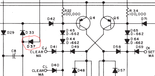
It was D37 on the R211 in slot PC10 that failed. Being connected to the base of Q4 would explain why this flipflop could not be changed.

1723902640126.png
 
We looked at core memory today.

All of the (0) and (1) bits of the MA are getting to the G209 Memory Selector FlipChips in the memory.

Pressing EXAM yields non-deterministic MB results. Most of the time addresses ending in 0,1,2 and 3 yield all zeros.

We looked at the READ and WRITE signals, and found that sometimes we see a READ and then both a READ and WRITE at the same time. We eventually found glitches on the T2B signal coincident with the edges of the READ and WRITE signals that would sometimes trigger an extra MEMORY START signal and therefore an extra READ signal. Connecting a 'scope probe to the T2B reduces the number of extra MEMORY START signals. Maybe we will add a capacitor to ground on the T2B signal as a temporary fix.

The INH voltage is 29.8VDC, and the R/W voltage is 46.4VDC. Both should be between 27VDC and 37VDC, so we need to look at the R/W voltage regulator.
 
Last edited:
We looked at all of the signals in the Inhibit and Sense circuits. Everything looks reasonable. We didn't see any extra T2B or MEMORY START signals today.

I guess we need to dive into the R/W voltage regulator next time.
 
Back
Top