• Please review our updated Terms and Rules here

Commodore PET 4008 with strange issues?

It makes sense too, because the original MOS 2114's are generally defective now, but those NEC ones are usually ok !
 
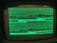
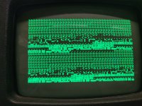
Well this is strange. I got back to the workshop today and thought I'd swap each concurrent RAM IC to see if there's any different result - specifically, if the "g"s move position, which I'd assume would indicate that one one of the eight ICs I purchased functions.

As far as I can see, the positions that pass haven't changed at all between the two tests (I've attached a before and after image, I'd specify the order but they seem the same so I'm not sure it matters)

IMG_20240610_130516__01.jpg
IMG_20240610_130201.jpg
Possibly badly soldered sockets? I can check continuity but they all seem alright. Strange that their contents are the same too, and seems to hold (at least in places) increasing numerical symbols. Perhaps the PETTEST ROM's socket isn't working any more?
 
If the CPU pin 7 (SYNC) is still pulsing, the PETTESTER ROM and socket is fine.

If you have swapped the DRAMs around (and you are swapping the DRAMs on the correct 16K bank of memory) the problem must be related to either the data bus buffers or the address multiplexing.

It looks like address $00FF is OK, so (if it is a data bus buffer) we have some bits stuck high.

Remind me, which PET are we repairing? I have so many on the go at the moment...

Just going out for a walk...

Dave
I'll check the sync pin with the PETTEST installed tomorrow... ...er... later-

This PET is a CBM model 4008, I got lucky enough to have all the RAM slots in-tact so it's an early batch of that lineup.

I'll check the schematics later (I'll sleep eventually) to see if I can identify the data bus buffer ICs on my specific board - I may well have a replacement lying around in the workshop. If it is the buffer, that'd explain all of the machine's behaviour to date, given that it can't interact in any meaningful way with main memory but the rest seems good.

It may be worth mentioning if I didn't already that the ICs I used to replace the original TMS4008 RAM chips are TMS4116's, but the shunts are still set for 8k. I don't think that should be an issue if my understanding of the original chips is correct (one half defective 4116s?) but just in case I'm overlooking something obvious.
 
OK, I am awake now (just)so I will have a look after breakfast).

I will also see what the patterns are (g and b patterns and what PETSCII characters are returned for the b characters).

Dave
 
In the meanwhile, I thought I'd be "clever" and replace the memory buffers at UI10 and UI11 with some 74HC244Ns thinking they'd be compatible. Alas it won't get to the memory test now, so I'm assuming it's an issue with the propagation delay difference. I also tried a CD54HCT244F3A for the hell of it, but no luck. I'll order two replacement 74LS244s and see if that's the issue. It it doesn't get to the memory test with them, I'll assume I've damaged the board in soldering, but I can't see any faults in my sockets visually.
 
Ah, I was about to post some of my findings and save you some wasted time. The wife has been out this morning so I thought I would take the opportunity to tidy up my work room. This involved filling other parts of the house with stuff that would have incurred wrath and indignation had she been aware of it! Anyhow, what the eye doesn't see...

The errors indicate that buffered data bits D4 and D5 are stuck high - thus pointing the finger at I11 or E10.

However, the address bus multiplexers could also cause similar problems (E3 to E6).

Always read the data sheets and seek advice before replacing a part with something else other than the original.

Dave
 
Last edited:
Ah, I was about to post some of my findings and save you some wasted time. The wife has been out this morning so I thought I would take the opportunity to tidy up my work room. This involved filling other parts of the house with stuff that would have incurred wrath and indignation had she been aware of it! Anyhow, what the eye doesn't see...

The errors indicate that buffered data bits D5 and D6 are stuck high - thus pointing the finger at I11 or E10.

However, the address bus multiplexers could also cause similar problems (E3 to E6).

Always read the data sheets and seek advice before replacing a part with something else other than the original.

Dave
Ah, the curse of having hobbies. Best wishes with... surviving, on my behalf!

When the replacement buffers arrive, if no measurable improvement in the RAM test occurs I'll swap out the multiplexers. I do have some MC74HC157Ns that are theoretically compatible, but as was the case with the RAM buffer I'm not certain that the higher speed will work with the overall timing of the system - might have to order some SN74LS157Ns instead but they aren't overtly pricey so not the end of the world.

I socketed I11 and I10, might've knackered the original ICs in the process, so I'll socket E10 as well and just get 3 new replacements to be safe.

Cheers.
 
Before you start replacing parts, remind me - do you have an oscilloscope or not?

Dave
Yes indeed I do. I have a scope, meter and basic soldering / desoldering equipment, and a load of second hand assorted components like DIP sockets etc.
 
So, using your scope to take measurements is a much better solution than randomly replacing parts.

How much knowledge do you have of electronic schematics and the use of the oscilloscope?

I have a meeting now...

Dave
 
So, using your scope to take measurements is a much better solution than randomly replacing parts.

How much knowledge do you have of electronic schematics and the use of the oscilloscope?

I have a meeting now...

Dave
Ultimately I acknowledge that I am but a hobbyist and my knowledge is limited to what I've figured out on my own and what I've learned from folks like yourselves. If I had a graph indicating an expected waveform and a reference to roughly where on the schematics it is, I could probably check it.

I'd say I know the basic operation of a scope and can read a schematic acceptably, but I'm not a pro by any stretch of the imagination.

To be honest, when I got the PET, I thought it wouldn't be too far off repairing a 64 - I realise I was sorely mistaken. That said, I think I'm now seriously hooked on repairing machines where I actually have to use my brain a bit, though I understand by now that I was clearly under-prepared for doing so with this specific machine...
Come to think of it, sorry it's been such a tedious process for all of you, I know I haven't been figuring all that much out on my own. I owe all of you a great deal of thanks for putting up with my incompetence frankly!
 
We can guide you - but you will have to put some effort in - to help you to become more proficient with your oscilloscope.

On the assumption that this schematic matches your machine: https://www.zimmers.net/anonftp/pub/cbm/schematics/computers/pet/2001N/320349-5.gif proceed as follows.

Check the signals marked as RAn (where n is 1 to 7) directly on the pins of the multiplexer ICs E3 to E6 for the following frequencies:

RA1 500 kHz.
RA2 250 kHz.
And each subsequent RA number being half of the previous frequency.

Note that some signals are connected to two (2) pins. Check both pins...

These are the Refresh Address (hence the RA nomenclature) signals - and (if they are missing) some/all of the DRAM contents can evaporate!

Check pin 2 of E3 to E6 for the presence of a 1 MHz clock signal.

If you had a NOP generator fitted, you could also check the BAn pins for the correct frequency on E3 to E6. If you do not have a NOP generator available, just check the BAn signal pins on E3 to E6 for signs of activity.

Similarly for the MUX A signal on pin 14 of E3 to E6 - check for activity.

That covers most of the input pins. I would then check the signal level for pins that are connected to 0V/GND and +5V (just to make sure the power supplies are connected correctly). If you have a logic probe, I would suggest using that for the 0V/GND pins - as using a multimeter or oscilloscope to measure 0V is not a clever thing to do... What voltage would we read for the case where the pin is connected to 0V and the case where the pin is disconnected from a source of voltage...

Next, check the output pins of E3 to E6 on pins 7 and 9 for activity.

We can be a bit more selective later on monitoring the output pins for the 'correct' activity!

That should keep you busy for a while...

If you need some help regarding setting up your oscilloscope, just ask. Single channel, DC 1V/div and select a suitable timebase based upon either the frequency or by observation.

Dave
 
I believe that is the correct schematic yes, at the very least it seems visually identical to the service manual. I've been referencing that one myself since.

Thanks for explaining the multiplexers, quite frankly I've never encountered one before. I'll be sure to consult the datasheet (if I can find one) too, just to make certain I'm measuring the correct pins. On the point of the clock signal, I don't know if I mentioned it before, but I replaced the crystal oscillator quite a while ago as it was putting out wildly incorrect frequencies, so if the clock isn't correct on one of the ICs now something majorly wrong has happened!

Alas I don't have a NOP generator, the PETTEST is the only PET-specific diagnostics unit I've got at my disposal. If I'm ever fortunate enough to work on another PET further down the line, I'll doubtless invest in one so I can perform a bit of a more thorough diagnosis before taking to the board with a soldering iron.

I've got a logic probe lying around somewhere (though I rarely use it), I can find it and test the 0V connection. Mind, perhaps I'm being a bit dim but I'm not sure what signal to expect on that line, I was under the impression it just acted as a return line for the whole circuit. I'll check the +5V on each IC too but I know the +5V line is ok around the actual RAM ICs themselves from prior testing.

I should be fine with measuring the frequencies specific with my scope. I'm familiar enough that I can probably dial in one for measurement / inspection - I've been using it for a while now, but ultimately I'm not going to call myself outlandishly competent at any of it - I know I'm in the initial learning stage for certain, at least when it comes to the PET.
By the by, one of the channels on my scope is completely knackered (a digital issue alas) so as long as I can keep to single channel observation it'll be fine.

I'm a bit occupied with work for the rest of the week, but with any luck I'll be in the workshop again on Friday; if not, Monday. I'll let you know how I get on when I check the aforementioned then. Thanks again
 
If you look at the schematic for E3 to E6 you should see that some pins (other than the power 0V pin) is/are connected to 0V.

What we are doing with this test is to make sure that the PCB tracking is OK and that the pin(s) really are connected to 0V when they should be! If not, the IC will malfunction in operation.

It is a quick check, so worth doing - even if a fault like this is statistically small. It has been known...

Dave
 
Ultimately I acknowledge that I am but a hobbyist and my knowledge is limited to what I've figured out on my own and what I've learned from folks like yourselves. If I had a graph indicating an expected waveform and a reference to roughly where on the schematics it is, I could probably check it.
I recorded most of the signals that control the 4116 DRAM in the dynamic PET, might help you as a reference, they are in this article about finding defective DRAM;

www.worldphaco.com/uploads/DRAM%20MEMORY%20TEST%20SYSTEM%20FOR%20THE%20DYNAMIC%20PET%20COMPUTER.pdf
 
If you look at the schematic for E3 to E6 you should see that some pins (other than the power 0V pin) is/are connected to 0V.

What we are doing with this test is to make sure that the PCB tracking is OK and that the pin(s) really are connected to 0V when they should be! If not, the IC will malfunction in operation.

It is a quick check, so worth doing - even if a fault like this is statistically small. It has been known...

Dave
Ah I see, that makes sense. Thank you for explaining! I presume then that a low signal on those pins would indicate a solid 0V connection (not something I've had to measure before)?
I recorded most of the signals that control the 4116 DRAM in the dynamic PET, might help you as a reference, they are in this article about finding defective DRAM;

www.worldphaco.com/uploads/DRAM%20MEMORY%20TEST%20SYSTEM%20FOR%20THE%20DYNAMIC%20PET%20COMPUTER.pdf
That's really helpful too, might need it for diagnostics as I go about testing, so that I have something to compare to. I'll check it out...

...on monday, because it turns out that folks don't know what to not CO2 laser cut, and my workshop was filled with chlorine gas on friday! I managed to get an extractor on before being forced to leave, so it'll be clear by monday with any luck. I'll update you all when I can.
 
>>> I presume then that a low signal on those pins would indicate a solid 0V connection.

That is correct.

if the pin is floating, the logic probe should not indicate a logic LOW (unless it is a really cheap one).

Some people try and measure the voltage on the pin and, if they measure nothing, assume that is 0V (and therefore connected). Not necessarily so...

Dave
 
Commodore did not use any pullup resistors on the outputs of the DRAM IC's. Have a look at pdf pages 11 and 12 of the article I posted. It pays to know about this when interpreting defective bytes returned from the malfunctioning memory IC array, when trying to figure out which chip/chips are faulty. The idea of the article was to figure out which ones, to avoid unsoldering perfectly good ones.

I have a policy about removing vintage DIL chips from boards:

1) the most important part to preserve is the pcb.
2) only remove chips that appear to be highly likely defective on in circuit testing & analysis.
3) Unless it is a super rare unobtainium chip, destroy the chip by cutting off its legs close to its body with fine needle nosed cutters, then remove the pins one by one and add fresh solder and clear the holes with the sucker. Using a temp controlled soldering iron.
4) don't remove whole IC's for the purpose of testing, or any plan that they might be put back in the computer.

It is all about having less thermal and physical stress applied to the pcb, not saving the chips as a priority, unless they are very rare parts, then save them. The chips get saved by the process of testing and analysis in circuit, so that it becomes unlikely that good ones are removed by accident. It helps greatly if sockets are already fitted.

When chips are removed to save them, sometimes small areas of the pin surface is still stuck to the inside of the plated through hole and can pull pieces out or lift pads, unless the pins are completely free, which can sometimes be difficult, even with a good sucker. Though, when the pins are removed one by one, it is effortless to clear the hole with one attempt with the sucker, in most cases unless there is significant thermal relief around the hole.

Some years ago I used a de-soldering tool for 14 & 16 pin DIL IC's that heated all the pins simultaneously to extract chips intact. Overall though, it was more stressful for the pcb and occasionally caused some damage. I have similar tools too, but now I reserve these for surface mount IC's, where it is the safest way to remove them.

The reason I'm mentioning these things, is that if chip un-soldering for "testing or replacement" is used as a random repair methodology it can result in a total disaster. There can be introduced faults from pcb damage, unsuitable replacement parts etc. Then the faults on the board start to multiply. Once I helped fix a Pong pcb that had about 65 TTL IC's. The technician had replaced probably 40 of them on hunches. Still, the board remained faulty. After all of the damaged from this was rectified (which was a very large job and the pcb would never be the same), the original faulty chip was found (with the scope) as being one of the remaining original ones, but even if that had got replaced more than a few of the other IC changes into the process, the board still would not have worked due to introduced faults.

It is somewhat unfortunate that the presence of cheap logic IC testers have appeared, because it has encouraged some people to use these as a "repair tool" removing, testing, and re-fitting chips on vintage computer boards, which is non ideal from the perspective of pcb preservation. The testers are really better deployed testing old stock IC's prior to use, to screen out duds, rather than as a repair tool. There is also no guarantee that if a tester reports a particular chip as ok, that it will definitely work in the particular circuit location. Some testers also report chips as duds, when they are not too. I think it still remains true that to test an IC on a vintage computer board, the better place to test it is right there, in the circuit it is in, on the pcb, before concluding it is defective and removing it. For most of the common TTL logic IC's, it is a matter of seeing if they are obeying their truth table with the scope or logic analyzer.
 
Last edited:
Commodore did not use any pullup resistors on the outputs of the DRAM IC's. Have a look at pdf pages 11 and 12 of the article I posted. It pays to know about this when interpreting defective bytes returned from the malfunctioning memory IC array, when trying to figure out which chip/chips are faulty. The idea of the article was to figure out which ones, to avoid unsoldering perfectly good ones.

I have a policy about removing vintage DIL chips from boards:

1) the most important part to preserve is the pcb.
2) only remove chips that appear to be highly likely defective on in circuit testing & analysis.
3) Unless it is a super rare unobtainium chip, destroy the chip by cutting off its legs close to its body with fine needle nosed cutters, then remove the pins one by one and add fresh solder and clear the holes with the sucker. Using a temp controlled soldering iron.
4) don't remove whole IC's for the purpose of testing, or any plan that they might be put back in the computer.

It is all about having less thermal and physical stress applied to the pcb, not saving the chips as a priority, unless they are very rare parts, then save them. The chips get saved by the process of testing and analysis in circuit, so that it becomes unlikely that good ones are removed by accident. It helps greatly if sockets are already fitted.

When chips are removed to save them, sometimes small areas of the pin surface is still stuck to the inside of the plated through hole and can pull pieces out or lift pads, unless the pins are completely free, which can sometimes be difficult, even with a good sucker. Though, when the pins are removed one by one, it is effortless to clear the hole with one attempt with the sucker, in most cases unless there is significant thermal relief around the hole.

Some years ago I used a de-soldering tool for 14 & 16 pin DIL IC's that heated all the pins simultaneously to extract chips intact. Overall though, it was more stressful for the pcb and occasionally caused some damage. I have similar tools too, but now I reserve these for surface mount IC's, where it is the safest way to remove them.

The reason I'm mentioning these things, is that if chip un-soldering for "testing or replacement" is used as a random repair methodology it can result in a total disaster. There can be introduced faults from pcb damage, unsuitable replacement parts etc. Then the faults on the board start to multiply. Once I helped fix a Pong pcb that had about 65 TTL IC's. The technician had replaced probably 40 of them on hunches. Still, the board remained faulty. After all of the damaged from this was rectified (which was a very large job and the pcb would never be the same), the original faulty chip was found (with the scope) as being one of the remaining original ones, but even if that had got replaced more than a few of the other IC changes into the process, the board still would not have worked due to introduced faults.

It is somewhat unfortunate that the presence of cheap logic IC testers have appeared, because it has encouraged some people to use these as a "repair tool" removing, testing, and re-fitting chips on vintage computer boards, which is non ideal from the perspective of pcb preservation. The testers are really better deployed testing old stock IC's prior to use, to screen out duds, rather than as a repair tool. There is also no guarantee that if a tester reports a particular chip as ok, that it will definitely work in the particular circuit location. Some testers also report chips as duds, when they are not too. I think it still remains true that to test an IC on a vintage computer board, the better place to test it is right there, in the circuit it is in, on the pcb, before concluding it is defective and removing it. For most of the common TTL logic IC's, it is a matter of seeing if they are obeying their truth table with the scope or logic analyzer.

Perhaps you raise a very good point, and I suppose my approach to testing has been rather juvenile with retrospect.
When I'm able to return to the workshop, I'll see if I can actually narrow down the fault properly, by scoping the recommended lines for both the buffers and multiplexers, and where anything seems indisputably wrong I'll look to replacing it.
In the case of this machine, this is the first IC that I've perhaps unnecessarily replaced (hopefully not but we'll see) - the RAM I intended to socket anyway as finding spare 4108s is virtually impossible and I didn't want to limit my machine to 16K, and while I've been lucky enough to have a PET 4008 with its expansion RAM slots not hole-punched out, I feel almost obligated to do so (I'm sure there's plenty of PET owners who wish they could bump theirs up to 32K but have the tampered sockets). The ROM sockets I replaced seem to have had a positive effect, as since the screen has actually attempted to clear on boot - I suspect the original white ones had given up the ghost.

But yes, I will admit that I feel a bit of a fool for rashly socketting this IC specifically. It was, at least, a fairly clean job by my standard, so I don't think it'll have put too much stress on the board.
Mind, it has taught me a moral - I can't just go soldering and desoldering on a whim without gambling the health of my board, and with such rare machines it simply isn't worth the risk if not absolutely necessary. I realise that now.
Perhaps I'm a little too used to working on 64s where a hunch goes a lot further (as it's usually the same telltale ICs to blame) and the diagnostics tools / processes are so simple a child could probably do it. I realise it's instilled a lot of bad habits that I really need to break if I'm to work on other early machines. I don't need to merely look at diagrams, I need to understand and work upon what they show too, and that takes perhaps a bit more thought than overall I've given at some stages.

In evaluation, some ideas I've had haven't been entirely wrong, such as suspecting a faulty clock and RAM - the clock was indeed knackered, and in a way the RAM portion is faulty, but jumping to the conclusion that it was a faulty 4108 was wrong and not far shy of guesswork, with retrospect.

I agree with your perspective on IC testers too - I was half tempted to look into them when I first started this repair, as a manner of sanity checking, but concluded that complete trial and error was a poor policy, even then. I scare to think what the board would've looked like now if I had...

I realise that this PET probably won't be close to perfect when it's "working". Cosmetically, it's pretty solid after a good clean, but the inside started as a bit of a mess and will probably end the same (albeit cleaner), no thanks to me; it has taught me that perhaps it's for the best if I leave these first-generation machines to those with a tad more experience, knowledge and skill than I, for now...

That said, I'll be damned if I don't see this PET working as Commodore intended; at this point in a ridiculous sort of way I owe it to that poor machine.

Thank you for the advice, and I shall attempt to take heed of the anecdotes, if not for my own sanity for the sake of preservation and to do no more unnecessary damage.
Cheers
 
Back
Top