• Please review our updated Terms and Rules here

GSETUP regarding expanded memory for IBM 5170

ROM images sent.

The source BIN file came from Lo-tech's web page on the XT-CF-lite rev.2, at [here]. The XUB version is R566, which is very old, and has bugs (but not bugs that would stop the XUB splash/banner text appearing). You could get this going, then look at an XUB upgrade.

Mission 1 of 2: Presentation of XUB splash/banner text

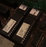
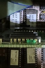
I tested the sent ROM images on my 5170 motherboard, of type 3, like yours. Into sockets U17 and U37. At power-on time, the XUB's splash/banner text appeared.

Mission 2 of 2: Ability of XUB to communicate with IDE circuitry

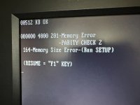
The XUB's splash/banner text indicated no master IDE device, which I expected, because I had no compatible XT-CF card plugged into the motherboard.

'Compatible = compatible with the controller type of 'XT-CF' that is configured in that copy of XUB.

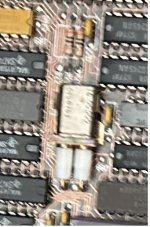
But I have a compatible card, a 'Sergey's XT-CF-Lite V4.1'. Card set to: EEPROM=D0000h, I/O=300h. I disabled the card's EEPROM via the applicable switch. Disabled because I did not want two copies of the XUB running (One at D0000 and one at E0000). I attached a wiped 32 MB CF onto Sergey's card.

I plugged Sergey's card into my 5170 motherboard, then powered on the motherboard. I saw the XUB find the 32 MB CF on Sergey's card. I then booted to a DOS boot floppy then proceeded to do the FDISK and FORMAT operations against the CF

After that, the 5170 motherboard was booting from the CF on Sergey's card.
I need to ask a question with regard to the U17 and U37 images sent. I have tried to load these using my GQ-4x4 read/writer. Every time I do so the log message is that the binary is too big and will be truncated. I tried these first on AM27C64 and again on an AM27128A chips with the same message displayed. I have 27256 but those are as big as I can get in terms of repeating the same code over a number of times. If the code is to be repeated 8 times then I would need a 27512 chip since the binary is 32-KB times 8 which would be 264-KB larger than the 256's I have. Is this correct or is truncation of the binary acceptable? Please advise. Thank you.
 
Check your mail, I gave you access.
I have it. I performed OCR on it, then hosted it at [here]. Thank you.

I need to ask a question with regard to the U17 and U37 images sent. I have tried to load these using my GQ-4x4 read/writer. Every time I do so the log message is that the binary is too big and will be truncated. I tried these first on AM27C64 and again on an AM27128A chips with the same message displayed. I have 27256 but those are as big as I can get in terms of repeating the same code over a number of times. If the code is to be repeated 8 times then I would need a 27512 chip since the binary is 32-KB times 8 which would be 264-KB larger than the 256's I have. Is this correct or is truncation of the binary acceptable? Please advise. Thank you.
The images are 'ready to roll' for 27256 (or W27E257).

I'll wait to hear from you.
A quick look at the manual reveals all of the other required information.
I'll post some test configurations shortly.
 
A quick look at the manual reveals all of the other required information.
I'll post some test configurations shortly.
It turns out that there is a DOS program supplied named CHSETUP.EXE
Answer questions it asks, and it will tell you what to set the switches to.

TEST #1

Motherboard providing 512 KB addressed 0 to 512 KB. Cheetah Combo providing 128 KB addressed 512 KB to 640 KB.

1. Run CHSETUP.
2. Select 'Cheetah Combo with 1.5M bytes'.
3. Answer as required for 'Do you want a printer port?'
4. Answer as required for 'Do you want a serial port?'
5. Press 6 (for 640K of base memory).
6. Press ENTER to accept 0 KB of extended memory.
7. Set the card's switches as displayed by CHSETUP.

8. Run GSETUP, or whatever, to configure CMOS SETUP to:
- Base/conventional memory = 640 KB
- Expansion/extended memory = 0 KB
 
I have it. I performed OCR on it, then hosted it at [here]. Thank you.


The images are 'ready to roll' for 27256 (or W27E257).


A quick look at the manual reveals all of the other required information.
I'll post some test configurations shortly.
If the manual helps someone who has similar card but no documentation of software to configure it.

Okay, 27256, got it, thank you.

Okay, I got your first test of the 128-KB for base memory no extended. I will advise on results of test.
 
IMG_5428.JPGIMG_5429.JPGThe Test 1 was a failure. I included some pictures from the CHSETUP. Of course all the memory chips still are on the card; that may account for the error, I don't know. The base memory was set back to the 512-KB size with 0-KB for extended memory in the AT's CMOS. I then powered down the AT and put in the Cheetah Combo card and got an immediate response from the Quadtel BIOS before I was able to even setup the CMOS. The error displayed for 1-sec Memory error and the switched to a second page showing Parity Check 2 again.

I looked up the Parity Check 2 error and found on some BIOS like that of say HP there is under their Advanced Menu a Bus Options command where the user can request Parity check as either enabled or disenabled. Quadtel doesn't have that parity enabling\disabling capability. I checked their conventional and advanced features for any parity related adjustments; none were found.

So, there is two possibilities. (1) The parity check 2 is coming from Quadtel BIOS and I need to remove Quadtel BIOS and return to the IBM BIOS and/or (2) That in addition to changing the BIOS I need to remove the memory chips from Banks 2 and 3 to meet the suggested memory total of 1.5-MB.
 
I re-installed the IBM BIOS this evening along with the XT-CF BIOS for U17/U37. So, I need to ask if there is supposed to a jumper initiated to let the motherboard know that BIOS U17/U37 are populated? Because when I turned the machine on, thhe memory counted off but the rest of the boot process was hung after the count off of the memory. Pictures show that both sets of BIOS's were seated correctly. Tommorrow, I'll have to pull U17/U37 and see if the IBM BIOS comes up without any problems then try re-seat the U17/U37 BIOS to see if they were causing the boot hang up. Before I re-seat them I am going to check them on the reader to make sure the binaries got installed correctly. While I have the U17/U37 out then I might try the Cheetah card again.
 

Attachments

  • bios's.jpeg
    bios's.jpeg
    169 KB · Views: 3
  • bios's2.jpeg
    bios's2.jpeg
    164.5 KB · Views: 3
I re-installed the IBM BIOS this evening along with the XT-CF BIOS for U17/U37. So, I need to ask if there is supposed to a jumper initiated to let the motherboard know that BIOS U17/U37 are populated?
No jumper/switch. It is as simple as 'plug the EPROMs in'.

Because when I turned the machine on, the memory counted off but the rest of the boot process was hung after the count off of the memory. Pictures show that both sets of BIOS's were seated correctly.
Odd. It cannot be due to the content of the EPROM's. If you had, say, accidentally programmed the wrong content into each EPROM, it would be the same as if you had not plugged in the EPROM's. I could populate a set of U17+U37 EPROM's with random bytes, and it would be as if I had not plugged in the EPROM's. For the POST to execute what is in the EPROM's, the first two bytes have to be 55 followed by AA, and, the 8-bit checksum of the entire 64 KB address space be 00. For random bytes, or U17+U37 swapped, the first two bytes will not be 55 followed by AA.

It has to be a hardware problem.

Tommorrow, I'll have to pull U17/U37 and see if the IBM BIOS comes up without any problems then try re-seat the U17/U37 BIOS to see if they were causing the boot hang up.
- Maybe re-seat them a few times, and look for pins bent up under the chip.
- And try different set of 27256 chips.

You have a type 3 motherboard, which, per [here], requires EPROM's that have an access time of 190 ns or better. I rule out 'out-of-spec access time' because the symptom would be the same as for corrupt/bad EPROM content.
 
Okay, I got your first test of the 128-KB for base memory no extended. I will advise on results of test.
This was expected to be quite straightforward.

chips still are on the card; that may account for the error, I don't know.
You informed CHSETUP.EXE that all three banks are populated, i.e. 'Cheetah Combo with 1.5M bytes'. Therefore, CHSETUP.EXE is expecting all three banks to be populated (with 256K-bit chips).

The base memory was set back to the 512-KB size with 0-KB for extended memory in the AT's CMOS. I then powered down the AT and put in the Cheetah Combo card and got an immediate response from the Quadtel BIOS before I was able to even setup the CMOS.
Expected. The RAM amounts found by the POST differed to the amounts in CMOS SETUP.

Because GSETUP forces a reboot, you will always see a RAM size type error during the process of adjusting RAM amounts in your 5170, irrespective of the order of things:
Order #1: Power off. Adjust physical RAM sizes. Power on. <---- 'RAM size mismatch' type error at this time. CMOS SETUP yet to be reconfigured to reflect new RAM sizes.
Order #2: Use GSETUP to change the RAM sizes in CMOS SETUP to reflect the future change that will be made to physical RAM sizes. GSETUP reboots system. <---- 'RAM size mismatch' type error at this time.
 
I looked up the Parity Check 2 error and found on some BIOS like that of say HP there is under their Advanced Menu a Bus Options command where the user can request Parity check as either enabled or disenabled. Quadtel doesn't have that parity enabling\disabling capability. I checked their conventional and advanced features for any parity related adjustments; none were found.
Disabling parity checking is like me seeing a warning light flashing on the console of my car, and in response, me disabling the light.

So, why might a motherboard BIOS allow the reporting of RAM parity errors to be disabled? Some reasons that I can see are:
- No parity chips fitted.
- Faulty 'parity generation and checking' circuitry.

The error displayed for 1-sec Memory error and the switched to a second page showing Parity Check 2 again.
You saw a "Memory" error then later, PARITY CHECK 2.

You are not being specific, and so I have to assume that by "Memory error", you are referring to a 201 error. As I stated earlier, if you see a 201 error, the needed information is in the 201 error - the PARITY CHECK 2 is superfluous. Run with the 201 error.

Yes, vintage computers can sometimes be a 'pain in the neck'. I imagine that, in the day, a lot of owners had their local computer shop do these kind of changes.

That in addition to changing the BIOS I need to remove the memory chips from Banks 2 and 3 to meet the suggested memory total of 1.5-MB.
You are using 256 K-bit RAM chips.
Each bank = 16 data bits x 256K-bit = 4,096 K-bit = 512 KB.
Three banks of 512 KB = 1.5 MB
 
I missed that you you did express that in a way within post #65.
The toilet paper.
Sorry about that being in the picture. I guess I am about ready to "flush" this machine. Actually, I have a head cold and I use toilet paper as a way to get rid of the unwanted mucus of the cold and I have to postpone until I feel better. I will rethink the EPROM problem by checking and re-seating them once I have checked their content as it compares to the responses you gave.
 
Last edited:
I was thinking about the speed of those 27256 chips. So, I checked and found they are way too slow, 250-ns which were greater than 190-ns. So, I ordered new ones much faster at 170-ns. So, while I recover I will pull those U17&U37's out and wait to the order arrives. Stay tuned. Mean time after the chips are out, I'll see if I can set CMOS to 640-KB base memory and 0 for extended memory using the GSETUP and see what is displayed again.
 
Process resulted in the same error using the IBM BIOS. I first, removed the U17/U37 BIOS mainly because the system was hanging every time I booted. As I earlier mentioned the U17/U37, which house the binaries that were provided were apparently too slow at 250-ns (new 27256 chips, 170-ns, are on order). I will update once these new chips are received.

I removed the Quadtel BIOS last week and re-seated the IBM BIOS this morning. I put in the Cheetah memory card using the configuration that was developed last week and then used GSETUP disk to reconfigure the CMOS for 640-KB and 0-KB for extended memory. As the attached picture, IMG_5437.jpg shows, I had set the Base Memory to 640, however, when rebooted the memory count stayed that same at 512-KB as shown at the top of the picture even though the Cheetah board was configured using the CHSETUP program included with the board. GSETUP was set to 640-KB however, the motherboard said 'Memory Error - Parity Check 2' as shown in the picture.

I believe there was a question as to the frequency of the clock on this motherboard. As the picture IMG_5436a.jpg shows the frequency is 16-MHz.

The error's encountered for the AST Rampage 286; configured with Base memory from 512 to 640 and 0 extended memory were directed at the address 80000 0001 Memory Error 201 and 164 memory size error.
Similarly, error's encountered with the IBM 512KB Memory Expansion Option as shown on minuszerodegrees website were at the address 80000 0001 Memory Error 201 and 164 memory size error. That board was setup with the 640 base memory and 0 extended memory as the others.

In every occasion the result is the same except for the Cheetah but essentially the system just rejects any change in the base memory. So, the next step is to adjust only the extended memory and leave the base memory alone and see what type of errors occur. Right now, it is my belief that the IBM type 3 motherboard that I am using was setup for one use where memory requirements were never going to exceed the limits of the 512-KB. You can see that even using the GSETUP to configure the motherboard for 640; the motherboard just defaults to the 512 and doesn't see anything beyond that setting or for that mater the Cheetah card itself. I have a Howard Sam's photofact of the IBM AT. The motherboard is a type 1 and not a type 3. So for me the photofact is useless for being able to diagnose why the motherboard can't see these memory cards.
 

Attachments

  • IMG_5437.JPG
    IMG_5437.JPG
    173.6 KB · Views: 4
  • IMG_5436a.jpg
    IMG_5436a.jpg
    79.4 KB · Views: 4
... being able to diagnose why the motherboard can't see these memory cards.
The POST, being informed that 640K of conventional memory exists, started to test it, and that test failed at the 512 KB address (80000h).

Cheetah card: 80000 4000 201 ------------------------------> bit 14 at address 512 KB
AST Rampage 286: 80000 0001 201 ------------------------> bit 0 at address 512 KB
IBM 512KB Memory Expansion Option: 80000 0001 201 ---> bit 0 at address 512 KB

A problem with only one of the 16 data bits, and that bit varies with card.

My IBM 5170 experience tells me that the cards are being seen. If the cards weren't being seen, you wouldn't have just one bit in error, you would have lots. You can prove that for yourself by having no card providing RAM in the 512-640K address space (and obviously, leaving CMOS SETUP set to 640K of base/conventional memory). If I do that on one of my 5170's the bit error pattern shown in the 201 error is FFFE (bits 1 through to 15).

If this was your motherboard faulty in a way that impacts on a single bit, then in the list of three cards above, it would be the same bit in error, not two different bits.

At a real stretch, for all I know, you could always be fitting the Cheetah card to a particular ISA slot that has a dirty/bad contact for bit 14, and always fitting the other cards to another ISA slot that has a dirty/bad contact for bit 0. Highly unlikely.

With your Cheetah card:

Visit all three banks, swapping the bit 14 and bit 12 chips in each bank. Does the 80000 4000 201 error then change to 80000 1000 201 ? If it does, you have a faulty RAM chip on that card.
 
Okay, let me investigate what you suggested here.

We also need to address the Parity Check 2 error as well.

I hope that our discussion will help others who are cloudy about memory as I have been.
 
The POST, being informed that 640K of conventional memory exists, started to test it, and that test failed at the 512 KB address (80000h).

Cheetah card: 80000 4000 201 ------------------------------> bit 14 at address 512 KB
AST Rampage 286: 80000 0001 201 ------------------------> bit 0 at address 512 KB
IBM 512KB Memory Expansion Option: 80000 0001 201 ---> bit 0 at address 512 KB

A problem with only one of the 16 data bits, and that bit varies with card.

My IBM 5170 experience tells me that the cards are being seen. If the cards weren't being seen, you wouldn't have just one bit in error, you would have lots. You can prove that for yourself by having no card providing RAM in the 512-640K address space (and obviously, leaving CMOS SETUP set to 640K of base/conventional memory). If I do that on one of my 5170's the bit error pattern shown in the 201 error is FFFE (bits 1 through to 15).

If this was your motherboard faulty in a way that impacts on a single bit, then in the list of three cards above, it would be the same bit in error, not two different bits.

At a real stretch, for all I know, you could always be fitting the Cheetah card to a particular ISA slot that has a dirty/bad contact for bit 14, and always fitting the other cards to another ISA slot that has a dirty/bad contact for bit 0. Highly unlikely.

With your Cheetah card:

Visit all three banks, swapping the bit 14 and bit 12 chips in each bank. Does the 80000 4000 201 error then change to 80000 1000 201 ? If it does, you have a faulty RAM chip on that card.
Your last line is the answer. I removed the 14th bit chip and swapped it for the 12th bit chip for the high banks 1-3 and saw the error move as your predicted to 80000 1000 201. Since the error occurred as you said; can we isolate the chip from this message or will I nave to move chips around until I find it? I am also just focusing on the Cheetah card for now. I'll deal with the others later. Thank you.
 
We also need to address the Parity Check 2 error as well.
I expect that that will disappear when the 201 error is addressed.

Your last line is the answer. I removed the 14th bit chip and swapped it for the 12th bit chip for the high banks 1-3 and saw the error move as your predicted to 80000 1000 201. Since the error occurred as you said; can we isolate the chip from this message or will I nave to move chips around until I find it?
The manual does not inform me of the address-from-bank relationship. So, swapping about chips is the answer.

Ensuring that we are 'on the same page':

In bank 1, swap back the bit 12 and bit 14 chips. If the bit error pattern in the 201 error goes back to 4000, then the faulty chip is the one now in the bit 14 position of bank 1.
If instead, the bit error pattern stayed at 1000, repeat the exercise for bank 2, and then if required. bank 3.
 
I expect that that will disappear when the 201 error is addressed.


The manual does not inform me of the address-from-bank relationship. So, swapping about chips is the answer.

Ensuring that we are 'on the same page':

In bank 1, swap back the bit 12 and bit 14 chips. If the bit error pattern in the 201 error goes back to 4000, then the faulty chip is the one now in the bit 14 position of bank 1.
If instead, the bit error pattern stayed at 1000, repeat the exercise for bank 2, and then if required. bank 3.
Your suggestion sounds like the better solution. I’ll try it today and see if I can isolate the defective chip and replace it. I’ll let you know.
 
You're going to love this one. I found that the chip in Bank 1 for what had been Bit 12 moved back to Bit 14 displayed the old error of 80000 4000 201. So, the chip was defective. I replaced the chip thinking, did we get them all; not quite looks like there is a new error message 80008 1100 201. Now the 1100 is signaling bit's 12 and 8 as the sources for new error's. However, it's the 80008 that has me confused. Is the message saying that I have two errors one in the high bank and one in the low bank?
 
Last edited:
Back
Top