• Please review our updated Terms and Rules here

Heathkit H11A Gett'er Working Thread.

Alright, so RAM cards. All the ones I have are 16 bits. Which is fine, but iirc I'll have to have a 22-bit memory of at least 1mb if I put the 11/73 card in and get it booting 2.11BSD.

After some head-scratching and reading of various existing designs, I think it would be not-impossibly-hard to put together a memory decoder with 74LS series logic, using LS240s for bus transceivers, LS273s for latches, and a small assortment of gates for decoding. It appears that the only critical timing requirement would be a small delay on the rise of RPLY, to give the data time to stabilize before it is consumed. I think this could be accomplished with an RC circuit into a gate with a schmitt trigger input, or one of those little 8-pin Maxim delay line units if an RC circuit isn't precise enough. With 4 or 5 jumpers, it should be possible to design a card that can take a pair of AS6C62256 32k x 8 SRAMs (for 64k on a 16-bit qbus system), a pair of AS6C1008 (for 256k on an 18-bit system), or 2, 4, 6, or 8 AS6C4008 (for 1, 2, 3, or 4mb on a 22-bit system), all using the same socket footprints.

The most annoying part will be filtering out segment 7 in the address decoding so that the memory does not enable while the IO segment is being accessed.

It would be possible to put all the latching and decoding on a small 5v CPLD, or maybe even a couple 22V10s, but that seems kind of cheaty and too anachronistic. And I guess others who might want to build one might not have a programmer for that stuff.

Those of you who actually know what you are doing (unlike me, lol), does this seem viable?
The signal BBS7 is used to decode the IO space. Add it to your decode logic to exclude IO.

joe
 
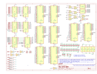
Here is what I've hacked together. There are doubtless mistakes that I haven't caught or thought of.......

OCFCO_QRAM.png
General Operation
-----------------

U1-U8 are Alliance SRAMs. They can be installed as a pair of AS6C62256 in bank 0 for a 64k 16 bit system, a pair of AS6C1008 in bank 0 for a 258k 18 bit system, or in 1-4 pairs of AS6C4008 for a 1, 2, 3, or 4mb 22 bit system. Jumper settings, provided on the schematic, serve to tie the unused address lines low and disconnect them from the bus (as the 11/2, 11/3 and maybe some others use these lines for other purposes), and to reconfigure pin 30 of bank 0 to provide CE2 or Vcc to the 32k and 128k chips, instead of A18.

/BINIT is asserted on system reset, and clears the latches.

FIXME: Do we also need to clear them on the falling edge of SYNC?

The QBUS signals are buffered through a pair of 74LS640 8-bit inverting bus transceivers, a 74LS240 8-bit inverter, and a 74LS14 hex inverter. LS14s could probably have been used in place of the LS240, but using the LS240 made drawing the schematic easier.


Address Latching Cycle:
-----------------------

The address is latched at the beginning of the bus cycle, regardless of whether it is a read or write cycle. The bus master drives an address on /BDAL0-/BDAL21. If this address is within the top 8k of the lower 64k address space (the peripheral IO segment), the bus master also asserts /BBS7.

On the rising edge of SYNC: A0-A21, /BS7, and the original inverted version of /A0 (this saves a gate later) are latched into a triplet of 74LS273 8-bit registers.

After at least 100ns, the bus master then clears the address from DAL0-DAL21, in preparation for the second half of the bus cycle. The second half of the bus cycle may be a read, a write, or a read-modify-right (a read followed immediately by a write to the same memory location, without releasing SYNC).

RAM chip enable is provided by a 74LS139 dual 2-to-4 decoder. A20 and A21 are decoded into a bank select, and the enable line is used to select between the low byte, the high byte, or both bytes (the whole 16-bit word). Details on the high/low bank selection can be found below.


Write Cycle:
-----------

The bus master places the data to be written on DA0-DA15. After 100ns, the DOUT and (if it is an 8-bit write) WTBT.

U16 handles the high- and low- byte enables. If /BS7 is low (an access to the peripheral IO segment), neither byte may be enabled. Otherwise, if WTBT is false (full 16-bit write) or A0 is high or low (depending on which half of the LS139 is being enabled), the 2-to-4 decoder is enabled and the a low signal is produced on the appropriate /CE (chip enable) line(s) for the RAM.

U17B generates a /WE (write enable) signal for the RAM, if /BS7 (IO segment) is not asserted.

With /CE and /WE both asserted on the appropriate banks of RAM, the memory latches the values presented on its data lines into the address pointed to by A1-A19.

The /WE signal passes through and is inverted by U17C. An RC circuit on the output of U17C causes a short delay as capacitor C0 charges until the voltage rises high enough to trigger the input of U15E. This delay gives the RAM time to store the data. When U15E triggers, it pulls /BRPLY low, signaling to the bus master that the data has been stored in the RAM.

In response to BRPLY, the bus master releases DOUT. BRPLY is released as a consequence, and then the bus master releases SYNC.


Read Cycle:
-----------

Read cycles are always a full word wide. WTBT is never asserted during a read cycle. As such, as long as /BS7 (IO segment access) is false, both 2-to-4 decoders are alwayys enabled. A20 and A21 are used to produce /CE (chip select) signals for the appropriate pair of RAMs.

The bus master asserts DIN, and as long as /BS7 (IO segment access) is false, an /OE signal is generated on the output of U17A.

With /CE and /OE both asserted on the appropriate banks of RAM, the memory presents the value stored in the address pointed to by A1-A19 to DA0-DA15 on the near-side of the bus transceivers.

The /OE signal passes through and is inverted by U17C, and a RPLY signal is generated in the same way as during a write cycle. Additionally, /BUS_OUT is asserted, which changes the direction of the LS640 pair, allowing the data from the RAMs to make its way onto the system bus.

The bus master consumes the data, and then releases DIN. BRPLY is released as a consequence, and then the bus master releases SYNC.


Potential Issues:
-----------------

This card does not make use of the +5B battery backup lines, nor does it disable chip selects in the event of power failure to preserve memory contents in the face of undefined bus signals. However, since most QBUS machines these days are only operated as a hobby, I don't think this is much of an issue.

The card decodes and drives the bus during reads throughout the entire memory map (excepting of course the BS7 segment). As such, it will conflict with any other memory cards installed in the system even if you don't install all eight AS6C4008s. If you are using a CPU with built-in RAM, that built-in RAM will have to be disabled. I do not have any such CPUs, and I have no idea if the built-in RAM on such CPU cards even *can* be disabled. So if this is a major issue then please let me know and we can figure out how to add some additional logic to mask off certain segments or something.

I wanted to do this with discrete logic and all through-hole ICs (because muh anachronism). I haven't even thought about laying out the board yet though. It may not all fit on a dual-height board. Our options in that case could be to make it a 2mb maximum card and add a jumper to select between the high or low 2mb (so you'd run two card in your system if you wanted 4mb). Or we could put all the decoding and latching on an ATF1502 or a couple 22V10s or something, although I'd hate to do that! Not everyone has the equipment to program that stuff.
 

Attachments

  • Theory_of_Operation.txt
    5.7 KB · Views: 4
Do you think I need to clear the latches on the falling edge of SYNC, or do you suppose it will work alright as is?

I'm also thinking about jumper(s) to inhibit the first <n> K of memory. The added circuit would tie into the way BS7 inhibits the RAM when the IO segment is accessed. This would hopefully allow people to run it alongside the built-in RAM of some of the CPU cards, which I imagine is probably a good bit faster than qbus memory.

Or maybe it's arrogant of me to assume that some other folks might want to build this thing too, once I get it working.

I have the edge connector, handle mounting holes, and edge cuts laid out in kicad, but I want to get the schematic as finished as possible before I lay it out.
 
Last edited:
The address latches do not need to be cleared at all. Just latch the address using SYNC (inverted BSYNC as you do). See also my version of a Q-Bus Memory Card . This one is mostly SMD mainly because the only 1Mx16bit SRAM for 5V I could has an SMD package. There is also a 2Mx16bit SRAM but only for 3V3.
 
Nice card. Yours is way more elegant than mine. XD

I still wanna do it the hard way though. Because muh anachronism.

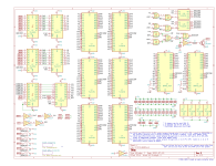
Here's my rev 2. Fixed some misplaced labels, added a subsheet that just has the edge connector and mounting holes on it (not pertinent to the circuit), and stuck a 2n3904 on /BRPLY as an open collector driver. I haven't done all the math, but I suspect that I'll need to futz with the RC values until the timing looks about right. output.png
 
Oops, there's another mistake. I needed to put that spare inverter in before the transistor so it would see a high value. Jeeeeeez.....

Anyway, what do you guys think about adding something so the lower X amount of memory can be turned off, to allow cpus with builtin ram and rom cards and such to work right? I was thinking I could stick an LS684 in there with a bank of dip switches or something, and then combine the P>Q output with BS7 to inhibit the card when the disabled areas of memory are accessed.
 
Anyway, what do you guys think about adding something so the lower X amount of memory can be turned off, to allow cpus with builtin ram and rom cards and such to work right? I was thinking I could stick an LS684 in there with a bank of dip switches or something, and then combine the P>Q output with BS7 to inhibit the card when the disabled areas of memory are accessed.

… woah. It had never occurred to me to use a magnitude comparator like this to set the lower bound of an address decode, that’s a great idea. I got completely snowed under at work and let the 16 bit ISA RAM expansion project I was working on completely fall on the floor, I think I need to get back to it before this falls out of my head because it sounds like a great way to tack “high resolution” start address selection for the XMS block onto the design while saving some GAL logic for other functions.

(I can land a bank of dip switches on the comparator and have it digest them instead of wasting the inputs on the GAL. For my purpose a ‘85 might be enough; cheaper and easier to find.)
 
I need to read up on how the boot roms work on these things. It seems like people always put their memory in from the bottom up, but if the root roms have to hang out somewhere weird so they match the reset vector, then that will have to be dealt with...
 
Yep, 173000 (or 17773000) would be the 'standard' location. Normally, the CPU can be configured to power-on jump to this address.

Dave
 
Hi Lee,

I completely understand the anachronism stuff. The main reason my card is SMD and rather small is that prices for PCB in full Dual Width Q-Bus Format are very expensive, at least here. Although the 2N3904 seems an elegant solution I recommend to use a 74F38 (yes the F Version, they have very low fan-in and high output current capability which almost matches Q-Bus requirements) or a 74S38 which was also often used in real hardware.

Instead of a comparator you can also use a full-adder.

I viewed some of your youtube videos and saw that you elaborated on the SASI card. Be aware that this not a general Q-Bus to SASI interface. I suspect yours is a SDC-RVL12 interface. This originally interfaced to a XEBEC S1410 formatter that interfaced to one or two MFM Harddrives. As seen by the PDP-11 this is an RLV12. I have an almost identical card, from Plessey and not SDC but jumpers are at the same place, and it took me some time to figure out how it can be made to work. For more information see the description of my Plessey System , at the bottom is the conclusion how to use it with a SD2SCSI V5.0. It even includes some autoboot features and so you do not even need a bootrom, it comes with the option to activate a bootrom so you can boot from the first UNIT of the RLV12 controller when you power-on your system.


Peter
 
One of my favorite lines from one of my favorite movies is:

"Now eventually you might have dinosaurs on your, on your dinosaur tour, right?"

So......

As the owner of a non working H11, I'm kind of curious.......

;-)
 
Hi Lee,

I completely understand the anachronism stuff. The main reason my card is SMD and rather small is that prices for PCB in full Dual Width Q-Bus Format are very expensive, at least here. Although the 2N3904 seems an elegant solution I recommend to use a 74F38 (yes the F Version, they have very low fan-in and high output current capability which almost matches Q-Bus requirements) or a 74S38 which was also often used in real hardware.

Instead of a comparator you can also use a full-adder.

I viewed some of your youtube videos and saw that you elaborated on the SASI card. Be aware that this not a general Q-Bus to SASI interface. I suspect yours is a SDC-RVL12 interface. This originally interfaced to a XEBEC S1410 formatter that interfaced to one or two MFM Harddrives. As seen by the PDP-11 this is an RLV12. I have an almost identical card, from Plessey and not SDC but jumpers are at the same place, and it took me some time to figure out how it can be made to work. For more information see the description of my Plessey System , at the bottom is the conclusion how to use it with a SD2SCSI V5.0. It even includes some autoboot features and so you do not even need a bootrom, it comes with the option to activate a bootrom so you can boot from the first UNIT of the RLV12 controller when you power-on your system.


Peter


Thanks for the info!!

Yep, that's exactly what card it is. I actually have almost enough stuff to assemble a 2nd PDP-11 once the H11 is all shiny and happy, so I was hoping to be able to use that SASI card in it.
 
One of my favorite lines from one of my favorite movies is:

"Now eventually you might have dinosaurs on your, on your dinosaur tour, right?"

So......

As the owner of a non working H11, I'm kind of curious.......

;-)


What's wrong with yours? I am pretty sure that this one actually works since I fixed the power supply, or at least "works enough to get somewhere with". When I stick a KDJ-11 in the backplane, the mini-blinkenlights inform me that it's trying to work but can't find a console serial port. I haven't gotten any farther than that yet. Got distracted with this memory card. <_< I need to make some cables so I can hook a terminal to it. It uses these weird molex connectors rather than DB-25 connectors.
 
Mine suffers from a number of faults.

1. The formerly working and adjusted power supply now blows the fuse.
2. The two H11-5 serial cards talk to the world through that funny square Molex type connector you mentioned. I have the half that connects to the card but not the cable half.
3. United Parcel Smashers (UPS) did a number on my H27. Booth doors are cracked almost dead center and bent in about 1/4".
4. I have too many projects, not enough time, and this machine hasn't yet risen to the top of my "quick fix failed, deal with other stuff first" pile.

But I do keep an eye open for H11/H27 threads for clues and was hoping to see some on this one. Ah, well, we live in an imperfect world.
 
2. The two H11-5 serial cards talk to the world through that funny square Molex type connector you mentioned. I have the half that connects to the card but not the cable half.

Yeah, same here. I only have the bits that go from the card and mount in the square knockouts in the back of the case. I was planning to make up my own cables that go from the card to DE9, and try to make something (possibly 3d printed if I can figure out the modeling software) to put 2x DE-9s in one of those square knockouts in the back.
 
Yeah, same here. I only have the bits that go from the card and mount in the square knockouts in the back of the case. I was planning to make up my own cables that go from the card to DE9, and try to make something (possibly 3d printed if I can figure out the modeling software) to put 2x DE-9s in one of those square knockouts in the back.
For reference those are Molex .062" series connectors.
Sample supplier: https://shopintertex.com/itx-mlx0070-062-molex-plug-receptacle-contacts-15-ckt.html
To the plug add a pair of dongles for your favorite DE-9, DE-25, MMJ, whatever suits connectors.
 
Back
Top