Giles,
Check these schematics and parts layout sheets to see if this is a match with yours.
http://www.zimmers.net/anonftp/pub/cbm/schematics/computers/pet/2001N/index.html
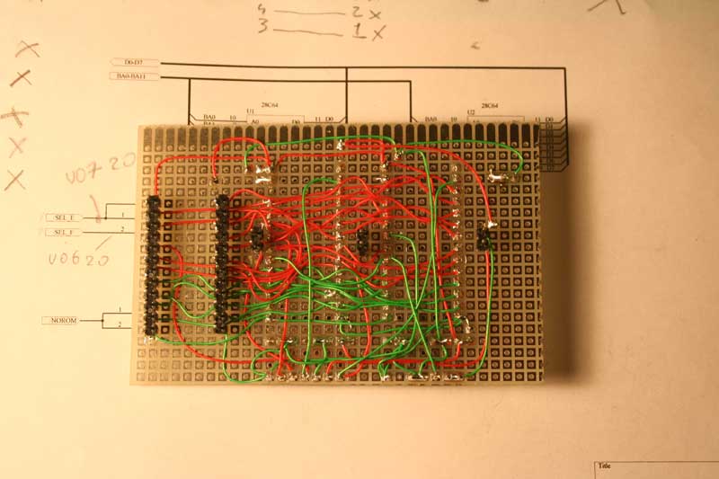
Yesterday much after midnight I had for the moment to "stop soldering and go bed" ...
I was getting the point I was making mistakes rather then good thing.
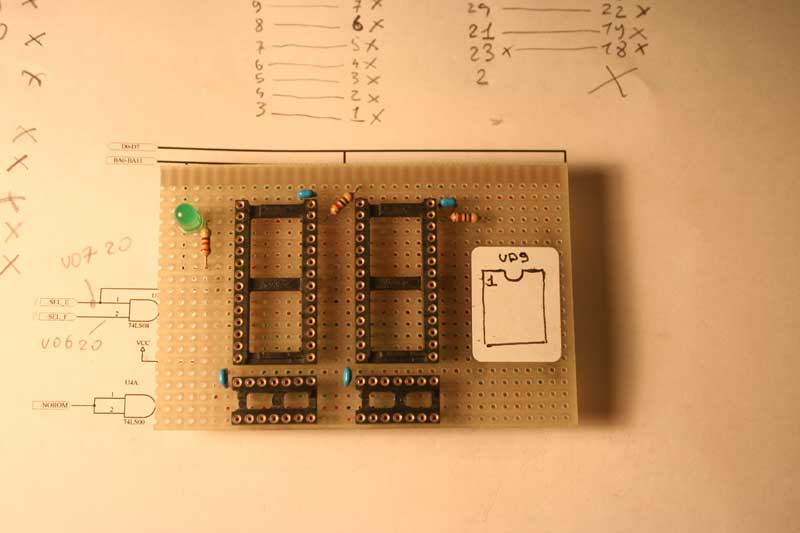
Ok looks like the schematics that applies to my board is this :
http://www.zimmers.net/anonftp/pub/cbm/schematics/computers/pet/2001N/320349-4.gif
Now note that the order of the roms is "F,E,D,C" starting from D9,D8,D7,D6 and they do not really show that rom 'E' has in reality A11 going into an /OE.
That 9,8,7,6 is different from the other schematics I had, I wonder in the first place if roms where in the correct order.
Then I did check with a tester where pins goes into starting from the 74154.
First of all .. yes .. there's not "that gate", pin /SELE is directly conneted to the rom in D8, so getting in from there misses the logic to disable the range E800 ( if you just get it without considering A11 ).
Second, it reconfirms the order 9,8,7,6 as F,E,D,C ..
Because I made my thing based on this schematics :
http://www.zimmers.net/anonftp/pub/cbm/schematics/computers/pet/8032/8032029-04.gif
I have to change a few more pins and connections.
This is just quite all the reverse of what I was thinking.
More update later ... after the coffee and the rest ..
")