dave_m
Veteran Member
Looking good so far!
Did you start the code using the Reset vector?
Did you start the code using the Reset vector?
| VCF West | Aug 01 - 02 2025, | CHM, Mountain View, CA |
| VCF Midwest | Sep 13 - 14 2025, | Schaumburg, IL |
| VCF Montreal | Jan 24 - 25, 2026, | RMC Saint Jean, Montreal, Canada |
| VCF SoCal | Feb 14 - 15, 2026, | Hotel Fera, Orange CA |
| VCF Southwest | May 29 - 31, 2026, | Westin Dallas Fort Worth Airport |
| VCF Southeast | June, 2026 | Atlanta, GA |
Looking good so far!
Did you start the code using the Reset vector?
was really not in fact correct?I have Wiley's Eprom Programmer, it does support 2716/32
Ok, so what you said in the beginning (#3 & #5) was really not in fact correct?
It proves anyway that definitely one of the 2114 was not well working, now we are writing some small programs to do a ram test and see if we find something else.
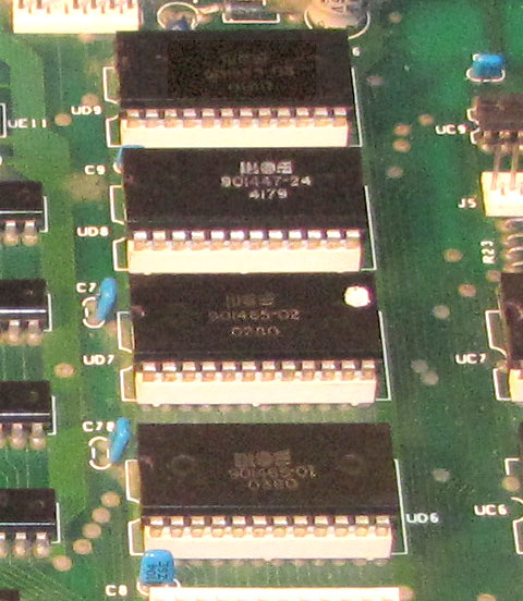
I assume you meant 901465-xx?[edit] I used the .bin files with the same numbers like in the ROM ( i.e. like 9014465-03, 01, 02 and 901447-24 .bin ) putting them in the order the should be.
I used the .bin files with the same numbers like in the ROM ( i.e. like 9014465-03, 01, 02 and 901447-24 .bin ) putting them in the order the should be.
I assume you meant 901465-xx?
So what order are they in then?
Originally Posted by GilesGoat
You know, much as I enjoy reading about your various tests and experiments it is a little frustrating when you don't read our replies or reply to our questions, so humour me and let me ask again:
Now that we finally know after two weeks and 85 posts that the ROMs are apparently OK, what order are you putting them in, i.e. which ROM # is in which socket? Not in the sequence above, I hope...
And a belated Christmas greeting to you and everyone still following this thread!
")

Originally Posted by GilesGoat
I used the .bin files with the same numbers like in the ROM ( i.e. like 9014465-03, 01, 02 and 901447-24 .bin ) putting them in the order the should be.
Well, the NOP generator that Dwight and I suggested would tell you that, but as you say, we'll have to wait and watch you do it the Italian way ;-)I wonder if there could be any failure in some of those 74244 address buffers, in particular the higher one that drives A8-A15 ..
I wonder again whether you're really correctly decoding the Exxx space; there is (or should be) NO ROM between E800 and EFFF....using that 'ff' trick I force it to fill all the space between E000 and F000 ( in the rom ) with 'FF' and have the code at the correct address.
I wonder again whether you're really correctly decoding the Exxx space; there is (or should be) NO ROM between E800 and EFFF.
True; it was meant to resolve this other issue of yours:However this does not tell me a thing I am going to test with my program, as the NOP generator makes the CPU span throught the whole 64K address space it will go into the I/O space as well.
and check some of the chip select decoding.I wonder if there could be any failure in some of those 74244 address buffers, in particular the higher one that drives A8-A15 ..
What happens when you disable the 6520 chip select?...Which is odd.
CS0 ( pin 22 ) of the PIA seems to be stuck in a '1' ( a bit dirty ) which is 2V, yes 2V not 5, in amplitude.