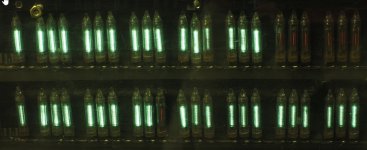
Update: Powers Up - VFD Lights UP! See pics and offer listing at: https://forum.vcfed.org/index.php?t...m-with-novel-vfd-display-panel-c1977.1249953/
| VCF West | Aug 01 - 02 2025, | CHM, Mountain View, CA |
| VCF Midwest | Sep 13 - 14 2025, | Schaumburg, IL |
| VCF Montreal | Jan 24 - 25, 2026, | RMC Saint Jean, Montreal, Canada |
| VCF SoCal | Feb 14 - 15, 2026, | Hotel Fera, Orange CA |
| VCF Southwest | May 29 - 31, 2026, | Westin Dallas Fort Worth Airport |
| VCF Southeast | June, 2026 | Atlanta, GA |
-
Please review our updated Terms and Rules here
You are using an out of date browser. It may not display this or other websites correctly.
You should upgrade or use an alternative browser.
You should upgrade or use an alternative browser.
Homebrew 6502 c1977
- Thread starter ic2024
- Start date
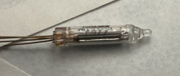
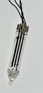
Update on the VFDs - Vacuum Florescent Display triode tubes/valves.
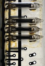
The display boards were salvaged from 36-bit mainframe CASINO project from early 1960s, then used in my Homebrew 6502 computer display.
Most used VFDs in this machine had NO markings! However found some spares used to maintain that original machine
that had two similar markings. CASINO was a 36-bit machine. I took a hacksaw to the PCBs, chopped them down to 32-bit.
Looks like ANODE/Plate voltage I used was 40v (needs physical verification).
Marking: two special symbols similar to "o" and uppercase "I", followed by 132D4 or 132C5
"Holland" 6977
These VFDs were first introduced in 1957.
6977 Info page:
Original Spec sheet:
Attachments
Eudimorphodon
Veteran Member
Bringing this thread back to life, since I *finally* got around to unboxing this last night; @ic2024 sent it over a month ago... all I can say in my defense was it was a pretty crazy October. I recorded a somewhat shambolic unboxing video that I'll try to get edited and posted; a little curveball that got tossed my way is the new phone I recorded everything on uses a codec that the video editor on my creaky desktop can't handle, so... nothing hours of downloads and conversions can't fix, right? Anyway.
To set the stage where we are at this point here's a photo of the card cage from the "for sale" listing for this machine:

I went through and pulled all the cards to see what was going on with them (don't worry, I have reference pictures where they were... and I *think* the bus slots are just wired straight across anyway, although I haven't completely confirmed that. Here's an initial set of findings:
"Keyboard/Front Panel":

"TV/KBD" and "SELECT 6000"

The backplane uses a 44 pin connector that's about 3.5" wide, and the card cage takes cards about 4.5" tall in total height. These appear to have been some kind of a standard, since several of the cards are built on off-the-shelf Vector protoboards; both the cassette and "front panel" board are unmodified Vector 3677s. When I was first looking at this I was speculating this could be STD bus, but a quick Google corrected that. (There was, interestingly enough, an STD *extender* included in the box, but it doesn't fit anything else.)
As I mentioned earlier, the one card in the cage that does appear to be a manufactured item is that RAM card. Here's what it looks like; it's a two-sided PCB with zero modifications on the card itself, and in one corner it has "(C) CCS 1976" etched into it. The board doesn't have any solder mask or silkscreening, but it looks like it *may* have plated-through holes so I don't think it was self-etched from a magazine. Does this board or the name "CCS" ring a bell with anyone? If someone recognizes this and knows what it was made for it might be a useful rosetta stone for trying to reverse engineer the pinout of the bus.


If anyone wants clearer pictures of anything let me know, I know these aren't great. If you're really a glutton for punishment I can take pictures of the backs of the protoboards so you can help reverse engineer the pinouts, but trying to do it by eyeball will be a lot like trying to untangle a plate of spaghetti just by staring at it....
To set the stage where we are at this point here's a photo of the card cage from the "for sale" listing for this machine:
I went through and pulled all the cards to see what was going on with them (don't worry, I have reference pictures where they were... and I *think* the bus slots are just wired straight across anyway, although I haven't completely confirmed that. Here's an initial set of findings:
- All the cards except for one (I'll get back to that) are hand wired on protoboard. Except for that one card none of them seem to be from a kit or anything.
- There is not a CPU card present, at least not one that fits inside the card cage. There's backplane extender board that looks like it could mate to the heavily modified OSI 400 CPU board that was included in the bundle; I'm curious if this was a setup used to prototype the other cards and there was intention to build an internal CPU for it? (Or, perhaps, there might be a second card cage/chassis that was positioned under this one and the two were cabled together?
- For the cards that are there their functions appear to be:
- VFD driver card. (This card is basically just a bunch of 7417 open collector buffers and resistors; I *think* it just reflects the status of the backplane bus lines up to the VFD with no special processing beyond that.)
- A cassette interface card built around a Motorola 6850.
- A 4K static RAM card utilizing 32 2102Ls. This is the one card that appears to have been repurposed from a commercial product or kit.
The next three cards are somewhat more mysterious:
- A 9" card that has two headers labeled "KEYBOARD ASCII" and "FRONT PANEL". The keyboard header has 9 pins, that could be barely enough for a 7 bit keyboard with strobe? The "front panel" has 7 pins and doesn't seem to mate up with anything that was included. The ICs on the card include 74367 hex buffers, 74157s, 74175s, etc... and two chips that say "931459 / MSI 7121" that I can't seem to find a sensible datasheet match for.
- A much shorter card that's mostly 74377s and 367s that has three dense headers on it that have labels "TV" and "KBD". These headers match a ribbon cable that's hanging off the heavily modified TV typewriter board that was included in the bundle... but there are three headers and only one cable.
- A mysterious board that's mostly NAND and NOR gates, a flip flop, and a 74154 4-to-16 decoder. It has three very thin wires hanging off of it, one of which has a label with "SELECT 6000" written on it.
"Keyboard/Front Panel":
"TV/KBD" and "SELECT 6000"
The backplane uses a 44 pin connector that's about 3.5" wide, and the card cage takes cards about 4.5" tall in total height. These appear to have been some kind of a standard, since several of the cards are built on off-the-shelf Vector protoboards; both the cassette and "front panel" board are unmodified Vector 3677s. When I was first looking at this I was speculating this could be STD bus, but a quick Google corrected that. (There was, interestingly enough, an STD *extender* included in the box, but it doesn't fit anything else.)
As I mentioned earlier, the one card in the cage that does appear to be a manufactured item is that RAM card. Here's what it looks like; it's a two-sided PCB with zero modifications on the card itself, and in one corner it has "(C) CCS 1976" etched into it. The board doesn't have any solder mask or silkscreening, but it looks like it *may* have plated-through holes so I don't think it was self-etched from a magazine. Does this board or the name "CCS" ring a bell with anyone? If someone recognizes this and knows what it was made for it might be a useful rosetta stone for trying to reverse engineer the pinout of the bus.
If anyone wants clearer pictures of anything let me know, I know these aren't great. If you're really a glutton for punishment I can take pictures of the backs of the protoboards so you can help reverse engineer the pinouts, but trying to do it by eyeball will be a lot like trying to untangle a plate of spaghetti just by staring at it....
Last edited:
Eudimorphodon
Veteran Member
... Continuing above, here's a picture of the OSI 400 CPU card.

As you can see, it's been pretty extensively gone over. In the picture of the "Keyboard/front panel" board in the previous post you can see the edge of the 44 pin extender card that was included in the box; it's my assumption that it was intended to mate with the card edge that's been attached. Haven't decoded the color codes on the resistors yet but I'm guessing they're to pull up the bus to stabilize it but... yeah, it's a bit unclear what's going on here. According to the manual I'd just started reading this card could take any of MOS 6501/6502 or Motorola 6800 processors; again, it's my guess it's set up for a 6502, but... I don't see any crystal for a clock, was this designed to run off of a multivibrator circuit?
I *think* the EPROM in the middle of all that spaghetti is an Intel 2708; it's very scratched up. As you can see it's sitting on a small scrap of PCB that has a voltage regulator on it, and there's leads going everywhere. I'm going to guess my TL866-II is *not* going to be able to read this thing; does anyone off the top of their head have a link to something like an Arduino sketch that might be able to read out its contents? I have a bench power supply I can get +5v and +12v out of, so I *should* be able to power it, although do I need to worry about any black magic like the order the voltages come up to avoid melting it?
This is the only ROM in the whole setup (other than the character generator on the TVT board), so I imagine it's probably pretty crucial to see what's on this if I want to understand how far this system might have gotten. I'll probably need to draft the help of a 6502 wizard to help deconstruct it.(*)
(The ROM sockets on this board were apparently intended for 1702 PROMs, so I suppose this one chip could hold twice as much as the intended devices. That doesn't necessarily rule out that it could just have the standard OSI monitor on it, though? If it was that then that should also reveal at least a little something about the I/O setup...)
Last edited:
Eudimorphodon
Veteran Member
According to the manual I'd just started reading this card could take any of MOS 6501/6502 or Motorola 6800 processors; again, it's my guess it's set up for a 6502, but... I don't see any crystal for a clock, was this designed to run off of a multivibrator circuit?
I’ve been reading the OSI 400 manual here, page A-3, and having a big “oh, duh?” moment; apparently you don’t *have* to have an external oscillator for the 6502 to operate, you can just create an RC network between the clock pins and it will free run?
After reading this I had a vague memory of a line in the ads for the Jolt 6502 that also mentioned using an RC clock with crystal timing optional, so… I guess maybe that mystery is solved? Maybe? I don’t suppose I’m lucky enough that someone on this forum had an OSI 400 and can confirm that this self clocking was utilized.
So… if this is actually what’s going on here, does anyone know if the modern WD65C02 CPUs will self clock like this? I don’t think I have a spare MOS 6502… I might have a Rockwell branded one from the early 80’s if I can find it, but I don’t know if that would behave like an original either.
Last edited:
Thanks very much for the investigation and first review! My memory is very patchy, however I'll try to fill in some gaps, but please don't rely on this ")
Thanks again for picking up this vintage story line!
- The 44 pin back plane bus should be wired straight across, not slot-specific. +VC and GND are top and bottom of the bus.
- The bus (TTL logic levels) on data and address went directly to the display using open-collector buffers with pull-ups to get larger voltage swings for the VFD grids.
- "Select 6000" is my hand-writing, but I have no memory of what this means

- Really no 6502 CPU in ANY of the 44 pin cards? This surprises me, I thought the CPU card, Memory card and VFD display the first ones, others added after. Is there a blank slot next to the VFD driver card where it should be? It's not much of a computer without a CPU!
- I have vague memory of the TVT mounted horizontally above the rack, perhaps between the rack and the front display. If so, that's completely missing or was just future plan.
- One of the cards should be my home-made video driver, displaying raw bit-level graphics using NTSC composite video (no character encoding).
- The cassette interface was early attempt at reel-to-reel tape storage.
- KBD may refer to the numeric keypad. This was used to enter octal program values into memory after cold start.
- I also recall there was a Cherry ASCII keyboard (bare key switches) with homebrew key-matrix scan, but this is gone.
- I have vague memory that the video sweep had the additional role of refreshing the DRAM bank.
- Sorry I can't remember how the OSI 400 CPU card was used. Most likely the EPROM was something different from what the board was designed for, so I created a daughter-board adaptor to sit on top of the old socket.
Thanks again for picking up this vintage story line!
CommodoreZ
Experienced Member
Oh boy, it's my time to shine! Full disclosure, I do not own an original OSI-400, I just have a replica from glitchworks.After reading this I had a vague memory of a line in the ads for the Jolt 6502 that also mentioned using an RC clock with crystal timing optional, so… I guess maybe that mystery is solved? Maybe? I don’t suppose I’m lucky enough that someone on this forum had an OSI 400 and can confirm that this self clocking was utilized.
However, before I built my replica, I dug up as many photos of authentic stand-alone OSI-400's and Challenger 65's that I could find for reference material. And none that I have seen use any sort of crystal or self-contained oscillator can for their main CPU clock circuit.


It just wasn't done, apparently.


And thus, the two other OSI-400 replicas I've found (the original made by @glitch and another one I spotted on youtube) both run from little feedback oscillators.


Thus, I built mine the same way, per tradition (although I'm running a 6512 in mine because I wanted to put that chip to work).

If I find a photo of a 400 board decked out with a crystal, I will be certain to report it.
Eudimorphodon
Veteran Member
However, before I built my replica, I dug up as many photos of authentic stand-alone OSI-400's and Challenger 65's that I could find for reference material. And none that I have seen use any sort of crystal or self-contained oscillator can for their main CPU clock circuit.
Huh. So yeah, I guess that was a method that was actually used for real applications in the wild. I've never seen it before, but I'll admit that every 6502 computer I've poked around inside before this one incorporated video hardware that ran synchronously with the CPU, and for that application I suppose it's pretty important that the computer run at a specific speed, not some ball park number derived from the analog components in the RC network.
")
Have you ever put a frequency counter on it and gotten an idea of how fast it actually runs? (And how stable it is.) Also curious if the duty cycle in particularly consistent...
Eudimorphodon
Veteran Member
Really no 6502 CPU in ANY of the 44 pin cards? This surprises me, I thought the CPU card, Memory card and VFD display the first ones, others added after. Is there a blank slot next to the VFD driver card where it should be? It's not much of a computer without a CPU!
Alas, yeah, no CPU in the chassis. There were two unpopulated slots between the VFD card and “Select 6000” (was next to the VFD) and the rest; next thing down was that “front panel” card, followed by the 4K static RAM card, the tape interface, and finally that buffer card that’s labeled to go to “TV” and “Keyboard”. If there was a CPU card not the OSI one it’s lost to history.
I have vague memory of the TVT mounted horizontally above the rack, perhaps between the rack and the front display. If so, that's completely missing or was just future plan.
I’m pretty busy today so I might not get to it “now”, but I’ll take some more pictures and dive into what’s going on with the TVT card. There are 10 wires connected around the DIP pin header labeled “I/O” that go through a ribbon cable that fits any one of the three headers on that buffer card; I assume that’s how you communicated from the CPU to the TVT, over parallel instead of serial…
There’s no obvious sign of any graphics interface functionality in what’s there, although some of the mods and the card edge on the TVT make me wonder if it’s possible you were leveraging its timing chains somehow? Do you remember if video generation on this graphics card was all “hardware”, or if it used software to some extent, like the TVT-5 for the KIM?
Eudimorphodon
Veteran Member
The 44 pin back plane bus should be wired straight across, not slot-specific. +VC and GND are top and bottom of the bus.
"Select 6000" is my hand-writing, but I have no memory of what this means
Had a few minutes to spare so I thought I'd share a thread I found to pull at.
Was looking at the cards, and I noticed something that makes me suspect that maybe the slots aren't entirely in parallel? (I haven't actually pulled the front door open to trace the backplane soldering yet.) Looking at the cards' connections to the bus it looks like only the static RAM card and the VFD driver have a "full" set of connections to the backplane; the "I/O" cards, IE, that buffer card that seems to cable up to the TVT and the tape interface, only have around a dozen lines actually connected. Here's photos of the card edges on both their front (component) and back sides:


Both cards connect mostly to lines on the "bottom" side (orientation when installed in the card cage) of the bus connector, with only a few straying up to the top side. That's not enough lines for these cards to be doing address decoding onboard, there's barely enough for the 8 data lines and a few control signals.
Interestingly, though, that mysterious "SELECT 6000" card is exactly the opposite; it connects exclusively to lines on the "top" side of the bus but has no connections to the lower end. Here's a picture of its component side; there's nothing on the back except for what I believe is a ground rail connection.

Obviously I still need to do a bunch of detective work to figure out the actual pinout of the bus, but this dichotomy of some cards looking like they *only* have data bus lines and a few control lines to them and this card that appears to *mostly* just be an address decoder (*) has me wondering if each slot might have a slot select (similar to an Apple II) and this card is the master? The markings on the piece of tape would make sense if each card were being assigned a 4K address slot...
(* This card also has a 7474 flip-flop, not sure what that's for...)
I have vague memory that the video sweep had the additional role of refreshing the DRAM bank.
No sign of a DRAM bank, alas. Only memory in the chassis is that mysterious "CCS" 4K SRAM card...
On the topic of that RAM card, I've been searching around and the closest hit I can find for a company name is a "California Computer Systems" that was mostly known for S-100 cards, but it looks like they were founded in 1979? Trying to find info about this may well be a dead end, but since it's just a RAM card reverse engineering it still might be a relatively easy way to figure out at least some of the bus signals.
KBD may refer to the numeric keypad. This was used to enter octal program values into memory after cold start.
I really feel like there must at least be a front panel/rack component missing; the keypad has a very nice Centronics connector on the end of its ribbon cable, but there's no mating connector on what I have. Guessing there used to be a pigtail that terminated from a panel to *one* of these cards.
Sorry I can't remember how the OSI 400 CPU card was used. Most likely the EPROM was something different from what the board was designed for, so I created a daughter-board adaptor to sit on top of the old socket.
Since there's no CPU card in the chassis I think maybe the best way to try to attack this is to trace out the memory card to get an least a rough stab at the bus pinout, and from there maybe I can trace backwards from the card edge that's been grafted to the OSI board and see if it looks like the OSI board was actually plugged into this chassis via the extender at *some point* and driving it.
The OSI board has provisions for serial I/O and a generic "put an IO chip here" footprint, and neither are being used, so I'm kind of wondering if it might make more sense to build from scratch a CPU card that fits the card cage than try to set up the OSI to drive it. I have some WDC6502S CPUs, flash memory, and SRAM lying around, I should be able to duplicate the OSI in half a dozen chips or so. But I should at least make a Hail Mary attempt to see if I can recover the contents of the EPROM on the OSI if tracing the lines indicates it might have control software for the tape interface or TVT in it...
Again, cry for help: Anyone think that "CCS" RAM card looks at all familiar? Or lacking that, any memories of a company that was making computer systems using a 44 pin card-edge bus that said card might be intended for? ...
WAIT. It looks like the MOS KIM-1 has 44 pin card-edge connectors? Could this be a KIM memory board?
Last edited:
cjs
Veteran Member
My first thought on seeing "SELECT 6000" was that it's a select for the $6000-$7FFF range, which is what you might use for I/O in a system designed for ROM at $8000-$FFFF and RAM starting at $0000. It also falls nicely out of obvious decoding arrangements for that, especially if you're intending to use 8K EPROMs. I used a similar arrangement in one bus I designed for an SBC with ROM, RAM and minimal I/O on the SBC itself, and cards for remaining I/O. This lets you have considerably less decoding on the I/O cards themselves.but this dichotomy of some cards looking like they *only* have data bus lines and a few control lines to them and this card that appears to *mostly* just be an address decoder (*) has me wondering if each slot might have a slot select (similar to an Apple II) and this card is the master? The markings on the piece of tape would make sense if each card were being assigned a 4K address slot...
So my guess, unless you find other more narrowly decoded select lines, would be that this is "I/O area select," and there might be further decoding on the I/O cards, either dividing down that 8K $6000-$7FFF range, or just using small pieces of it that get mirrored through the range.
Does the "SELECT 6000" line lead to one of the select pins on the '154 4→16 decoder/demux on that board, with some low address lines leading to other inputs on it?
Eudimorphodon
Veteran Member
My first thought on seeing "SELECT 6000" was that it's a select for the $6000-$7FFF range, which is what you might use for I/O in a system designed for ROM at $8000-$FFFF and RAM starting at $0000. It also falls nicely out of obvious decoding arrangements for that, especially if you're intending to use 8K EPROMs. I used a similar arrangement in one bus I designed for an SBC with ROM, RAM and minimal I/O on the SBC itself, and cards for remaining I/O. This lets you have considerably less decoding on the I/O cards themselves.
The tape with “SELECT 6000” is on a long wire pigtail; my working theory isn’t that the 6000 refers to the whole card, it’s that there was some external device sitting on the end of that leash that was intended to come on when the $6000 page is active. (Write to $6000h and the duck comes down?) Traced the pigtail and it is terminating on the “6” output…
The *simplest* scheme would be to just put this on the high nibble of the address bus and chop the address space into 4K chunks; that’s what a Commodore PET does… but it certainly *could* be more granular than that.
I need to start a document mapping things out, but I can also verify that several other of the *outputs* from the ‘154 terminate on bus pins. That pretty much makes it a slam dunk it’s acting as a decoder for other cards; I guess the question is if the bus is parallel across all slots and the cards are wired to their chosen select pin, or if the slot this card was in is “special” and cards decode depending on what slot they’re in. (Commodore machines commonly did the “pick a preset chip select” thing…)
Eudimorphodon
Veteran Member
Front panel - turn the two slot-pins 90 degrees to open, panel is hinged.
Yep. It was stuck when I tried to open it; I think the little dingus one of the slot pins goes into came loose and is spinning around, so I was putting off going after that until pulling the cards so maybe I could put pressure on it from the back.
syzygy
Veteran Member
Remember though, the Kim-1 has two 44-pin connectors. There were a number of KIM 1 memory expansion articles in Byte and Kilobaud ( eg., this one). It might be worth tracing out the signals.WAIT. It looks like the MOS KIM-1 has 44 pin card-edge connectors? Could this be a KIM memory board?
Eudimorphodon
Veteran Member
Remember though, the Kim-1 has two 44-pin connectors. There were a number of KIM 1 memory expansion articles in Byte and Kilobaud ( eg., this one). It might be worth tracing out the signals.
I read up on it after making that guess; the KIM basically has the CPU bus on one of those connectors, and the other is I/O from the 6530’s and some pre-decoded chip selects. The example in that article uses the decodes so it has to use both; you *could* make a memory board with self-contained decoding that just uses the top connector…
But I don’t know, that was probably a dry well in terms of dashing my hopes I might be able to find a manual for the board. Commodore sold “similar” 4K SRAM boards but they’re not the same shape, and I haven’t found any third party operating under the name “CCS” marketing their own expansion chassis for the KIM.
I probably won’t have time until the weekend, but my next step was probably to trace back the address and data lines from the 2102s on that memory card to the bus; that should give me at least 10, possibly 12 (if it *were* a KIM card that uses the pre-baked selects then it’ll have four of those instead of A10-11) address lines and the data lines. In the process it should become clear if it’s *not* a KIM board, but the mystery of “CCS” will remain.
Eudimorphodon
Veteran Member
Yep. It was stuck when I tried to open it; I think the little dingus one of the slot pins goes into came loose and is spinning around, so I was putting off going after that until pulling the cards so maybe I could put pressure on it from the back.
Was walking by it and decided it was high time to get it open; I don't know *what* was making it stick. It's like the retaining washer got hooked in the hole or something; I was in the process of unscrewing the whole bracket when it just decided to let go, no sign of why it was wedged.
That pretty much makes it a slam dunk it’s acting as a decoder for other cards; I guess the question is if the bus is parallel across all slots and the cards are wired to their chosen select pin, or if the slot this card was in is “special” and cards decode depending on what slot they’re in.
So I think I have a partial answer to this now:

At least some of the cards (the three I identified above as "I/O" cards) are using pin 1 as a slot select. See the crude green circles; each of several slots has a flying wire from pin 1 to a separate pin on the slot the "SELECT" card was in.
It's interesting how the slot that the Select card was in and the one next to it seem to also have a different arrangement of some of the other wires than the other slots. I guess I'm going to need to continuity test across the whole lot to see how this maps out. Referencing my pictures of where the cards were originally the third slot from the right was one of the two empty ones; I guess the other one was the one at the far end. That actually makes me think one of the cards (I'm going to guess the "TV/KEYBOARD" one) got moved, because it's one of the "I/O" cards with only a few pins connected (including pin #1), but when I received the box it was in one of the nothing-on-pin-1 slots...
syzygy
Veteran Member
But so too are your skills to create these boards so many years ago and do it with what was in your means. No embarrassment needed.You're doing an absolutely amazing job of deciphering unlabelled spaghetti! Embarrassed that my mediocre soldering/construction skills are finally exposed!
Robbbert
Veteran Member
- Joined
- Jan 10, 2019
- Messages
- 502
I have to admit, as soon as I saw CCS, it reminded me of a few non-working systems in MAME that were created by California Computer Systems. Officially, this company started in 1979 and lasted about 10 years, making plug-in S100 boards, single-board computers and other simple things. Your CCS board says 1976, so maybe they existed unofficially for a while? Or perhaps I'm muddying the waters? It's hard to know.