• Please review our updated Terms and Rules here

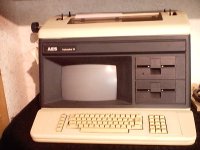
Lanier Model 103 "No Problem" word processor

In this instance, it would seem that the full size ship is being constructed inside the bottle, but only because the bottle has been made bigger on the inside.

--Phil
 
The EEPROM is fairly forgiving, in terms of programming. You can give it a single byte, or up to 128, I think, within the time window of "write"

I can get the parts put on order this weekend, unless you change your mind; breadboard it once they come in as proof of concept.

--Phil
 
Being as I'm not that hot with C# you may have to introduce some wait states on the logic for communication with the Arduino.

So long as that can operate at less than the bus speed, we should be good. The Arduino, when running the library functions performs buffering checks to ensure the lines are all correct before presenting the output.

In C# you can drive the lines directly without checking and thus work a lot faster. Let me know your thoughts.


--Phil
 
I have no qualms about which SRAM to use- so long as it's through-hold DIP I'm good. I'll let you pick. So far it's a wide open table because nothing's been purchased. Likewise the EEPROM if you wish to change it.

The Arduino is good up to +20V on each pin before it is damaged. I think. The "ready" signal if it is needed, once its address and data buses are stable is easy to provide.

--Phil
 
I confirmed that all the 74LSxx Plastic DIP chips are active production via the Texas Instruments website. No parts should be difficult to order when the schematics are done. Since I'm only addressing 4 registers in this design, I have to do more address decoding to select them. I'll use a 74'11 triple AND gate with three inputs each, to do the decoding. Basically if A2-A7 are high, and A8 is low, then A0-A1 select one of the four registers. I'll post some schematics next week.


Previously:
I did the 8K eeprom + 2K static ram changes to the schematics, system diagram and register map.

The original prom address block, 0000h-01FFh, it is now split into two 256 byte blocks; eeprom in the low half, 0000h-00FFh, and ram and the high half, 0100h-01FFh. The register block is in the top of the eeprom at addresses 00FCh-00FFh. It only consumes 4 bytes of each 256 byte page.

I've switched to 74'273 latches so I can clear them with a power-on-reset (POR#) or mode register bit to assure eeprom and ram always start on the same base page. It also assures that the flag register is selected (FLG#=0).


Previously:
Your suggestion to have the Arduino drive the cable lines directly is a good one.

The Arduino transfer during eeprom programming would probably be something like this:
The Lanier asserts a handshake signal requesting the Arduino to send a byte. The Arduino takes the next byte to be programmed and latches it into its shift register and then signals the Lanier that a byte is ready with a handshake line.

The Lanier then clocks 8 bits down the cable, reads the arriving byte and stores in a 128 byte buffer in the static ram. When 128 bytes are buffered buffered in ram, the Lanier temporarily delays another byte request and reconfigures to program-mode, copies the 128 bytes from ram to the eeprom and waits until it switches from busy to ready. At that point it requests the Arduino to send another 128 byte block as it repeats the process above, block by block.

Note that the eeprom has to be programmed by the Arduino to start with this firmware to thereafter program the eeproms in-circuit. So the Arduino will likely have to jumper into this board to run the program by the Arduino. I might add a connector to make that easier.


Previously:
The firmware to make the Lanier program the eeprom requires two pieces of code: (1) runs in eeprom and (2) runs in static ram. Ram allows firmware to be fetched while the eeprom is busy programming a 128 byte block.

Where Do.Rom is eeprom code and Do.Ram is static ram code:
(0) Do.Rom copies Do.Ram from rom, to static ram.
(1) Do.Rom downloads 128 bytes of new code from the Arduino into a ram buffer.
(2) Do.Rom jumps to Do.Ram where it changes to program-mode.
(3) Do.Ram writes the 128 byte buffer into the eeprom.
(4) Do.Ram waits until the eeprom is ready by looping on the BUSY flag.
(5) Do.Ram then changes out of program mode.
(6) Do.Ram jumps back to a Do.Rom entry point.
(7) Do.Rom exits if done, otherwise loops back to (1).

As noted previously, it possible that the Do.Ram code might also manage the download and buffering from the Arduino. There is only 128 bytes for code in the ram as it holds 128 bytes for buffer too. If there is codespace available, Do.Ram could be downloading a new buffer while monitoring the BUSY signal. The eeprom would likely be ready before the download is complete, but that's not a coding problem.


Previously:
Theory of Operation: The Lanier (Host) has these signals to interface in the prom socket:
A00-A08 to address 512 Bytes of original Prom space
CE# to select the board
D0-D7 to originally fetch|read the prom.

The host data bus connects to an internal data bus through a 74'245 transceiver to access four special registers. A08 selects the static ram when high and the eeprom when low. A00-A07 address a 256 byte page of either device.

The eeprom and ram blocks are independent, a necessary feature to allow the Lanier to program the eeprom while running the program in ram.

A mode register latches values to control the board. A flag register allows the Lanier to read status bits.
 
Last edited:
I've got the circuit done but the odd way the Lanier CPU card addresses the original prom needs to be revealed via schematic capture before I'll really know that the data will write into the chips on the board.

The problem is basically the T.I. 512 byte prom. It has address lines, data lines and one control line: CS#. We saw a little bit of the logic glue around that 74'48 (whatever) decoder they used. At some point we're going to have to capture that part of the circuit to be sure.

Probably all they did was delay the decoder chip select line until the RD# signal was valid so it didn't drive data onto the bus as soon as the address lines decoded that block of memory.

As this circuit addition does writes, I have to confirm that the CPU card doesn't disable that decoder during write cycles (just to prevent bad code or bugs writing data at the prom while the prom is writing data back at the bus. Many ways to clean that up of ignore it... I don't know which solution AES chose.

So, there is no reason to buy some chips if the Lanier card messes with this approach. Schematics from a retired AES employee would be ideal... but we'll likely have to do it the hard way. Not really a good time for me to be focusing on that.

An alternate trick would be to imagine a simple tester board that would give us the information or perhaps figuring a way to scope it out.

It might be that removing the DMA controller temporarily, and tying a DMA REQUEST line active, would get the 8080 to snooze on NOP instructions internally, allowing you probe the data and address bus with the Arduino. Removing the DMA controller assure it won't relinquish control back to the 8080 or that another DMA line takes priority over our choice. I really don't need to read the DMA controller chip that deeply unless I have to code for it.
 
Last edited:
I was considering that as an idea, and it's a good one. If the board is extended out to fit the same form factor, there is a nice un-screwable panel on the back of the case that could be removed to give access to flash etc.

I'll try start tracing the bus connectors at some point this week- have a large recap project going on right now.

--Phil
 
This is going to have to go on pause for a short while longer until a bunch of family and work stuff gets out of the way.

--Phil
 
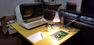
okay, have cleared a workspace for the machine, with access all around and power. It's a bit heavy for the table but it should do. Can get back onto it now..

--Phil
 
Great!

I'm doing a schematic capture on another system's board testing out the technique I think will make the Lanier boards more efficient to do. This other board doesn't have as many traces running mysteriously under chips as the Lanier boards, but the technique addresses all those hidden pieces and should organize piecing them back together, better.

Until then, some schematic information about the CPU card's address decode and signals on the bus could validate that rig design that is standing by.

Getting the bus information may allow the "rig" to be done on a sawed-off S-100 prototype board as the bus edge connector on both systems are the same. Just cut the left was right sides of the S-100 board profile to match the connector offset and card width and you have it. Of course this board will be shorter that the other Lanier cards but there will be plenty of room on the board.

Might have to start watching e-Bay for a S-100 Prototype Board.

I used one in 1979 to build a General Instruments AY-3-8910 programmable sound generator board (schematic plans published in various articles).
 
I saw a site that had S-100 prototyping boards available whilst I was thinking about expansion units. I'll see if I can dig it up.

If not I can solder (laboriously) flying leads onto the backplane and bring it onto breadboard for now.

--Phil
 
i recently acquired an AES Plus (aka 103), and found this thread by accident, when trying to find out more about it. Sadly, I have no disks, and haven't yet tried to power it on. I am suspecting that it will be in a similar shape to the one in this thread.
 
Paul,

Due to Life(tm) getting in the way, mine has sat on the desk untouched for the past half year. I need to get back to it- if I find a way to build an interface cheaply enough to boot something like CP/M, I'll post it here.


--Phil
 
My, oh my, oh my. Where did the time go?

I know where it went. Work, life, death, court, houses and lawyers.

However, I have managed, for the first time in two years, to gather up something resembling a work space (now in my new house, woo!) and have dumped the Lanier into a table, pulled the CPU card out and have made a start on making a circuit diagram.

I've also got a logic analyzer on its way, which may or may not assist in the undoing of this device.

20171020_212012.jpg

Here goes nothing.

Phil
 
Brings back memories of my Alphaplus 14:

aec_0009.jpg

It would only typewrite on the built in printer.. no sign of life onscreen and no attempt to boot. I talked to an engineer who worked on them and he told me finding boot disks would be impossible. Sadly I ended up getting rid of it in a move (took up too much space at the time) and wasn't all that interested given I'd been led to believe it was just a Word Processor anyway. Boy that thing was a beast!! Hope you get yours going!!
 
Looks to be much the same kind of machine. Can't see them deviating too much from the innards as this one has.

I'm going to try mock the boards up in kicad and go from there.

Phil
 
Wow.. Great thread. Obviously someone early on deleted all their posts or they were otherwise removed. Unfortunate, as you seem to be having a very one way conversation for the first 10 pages :)
 
Yeah, shame. I forget who it was who was commenting; it was a good while back. I guess they deleted their account for the system to not show their posts at all, rather than *deleted post* placeholders.

Phil
 
Back
Top