• Please review our updated Terms and Rules here

Neglected PET needing some love

That is the purpose of the decoupling capacitors. They should be mounted as close as possible to both the VCC and GND pins of the associated IC.

The decoupling capacitors hold a small charge. When the Integrated circuits 'switch' - they can draw an appreciable current for a very short period of time. This delta current is provided by the charge that has accumulated on the decoupling capacitor. If you do not have the decoupling capacitor, this current has to be supplied by the VCC and GND tracks. The longer/thinner these tracks are, the more pronounced the voltage drop will be across the tracks. These switching currents will, therefore, be 'conducted' around the rest of the circuit as electrical noise on the power planes.

On a PCB we had at work, we were measuring 1.2 Volts (yes Volts) of drop across a GND and VCC track that had an incorrect decoupling capacitor fitted. Admittedly it was a high-power bus driver - but the event is noteworthy all the same. The circuit designer was (basically) an idiot. Solved by making a solid GND and VCC plane and directly bonding the IC power pins to the planes via thermal reliefs. This is a 6-layer board though.

My personal preference is to make a complete ground plane and to connect the decoupling capacitor as close to the IC VCC pin as possible and the other side of the capacitor to the GND plane.

My thoughts...

Dave
 
My personal preference is to make a complete ground plane and to connect the decoupling capacitor as close to the IC VCC pin as possible and the other side of the capacitor to the GND plane.

My thoughts...

Dave
Agree. Most boards are better off if one side of the pcb dedicated as a ground plane. Usually the top surface, Then anything which requires a ground just acquires it there. Simple to do.

Though, many designers of analog RF gear didn't go to a ground plane unless they were making gear that operated over 30MHz. For example, a typical medium wave and shortwave radio of yesteryear had no ground plane on the pcb, unless it was professional equipment.

The interesting thing though, about digital logic, it operates often at radio frequencies and the switching transients can be well into the tens of MHz region in a vintage computer and into the UHF & GHz region in a modern computer.

So it does pay to think of the humble digital logic board, like it is an RF board; use ground planes and ample capacitive bypassing for the best results. And if you are thinking of sending digital signals to other places on other boards, with ribbon cables etc, consider series 22R to 33R carbon resistors in series with each conductor to act act RF stopper and make sure the cables are terminated at the far end. These resistors work because they form a mild LPF with the input capacitance of the circuit the cable is feeding.
 
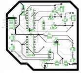
Alright here's the next revision. In this CAD program (DipTrace) I can make a "Copper Pour" but it doesn't show it as being connected to anything. For now I've just made one big fat trace around the whole board.

petCompV3.jpg
 
Alright, I finally got the PCBs and soldered in all of the components this morning. I guess I'm ready to test it out. I could have sworn there was a pinout of J7 at http://www.zimmers.net/anonftp/pub/cbm/schematics/computers/pet/8032/index.html but I must be blind because I'm not seeing it.

I did find one here: http://www.zimmers.net/anonftp/pub/cbm/pet/manuals/8296supplement/imgs/j7.gif which is probably the same as my 8032, even though it's under "8296 supplement".

If that pinout is correct then the one thing I'm lacking is 5 volts, which I guess I could take off of a chip or a cap somewhere, any suggestions on the best place to pull that from?
You could take it from any of the power pins of the logic IC's which is pin 14 or pin 16 of the package (Unless its something like a 7490 or 7493 with the power on another pin). Or from the 5V regulator output area. When I built an add on board for my PET I used the GND and +9V connections on the pcb plug J11, but that required a 5V regulator on the add on pcb.
 
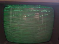
Well the good news is there is some sort of signal but it's definitely not right:
20230210_135917.jpg

The only adjustments on the monitor are brightness, contrast, vertical hold and vertical position.
If I pop the back off, internally, there are pots for:
focus, h.hold, h. sub hold, v.lin, and +b.adj
 
That looks (initially) like a horizontal hold thing to me.

Don't forget that you have 'inversion' options for both horizontal and vertical drive signals...

Dave
 
That looks (initially) like a horizontal hold thing to me.

Don't forget that you have 'inversion' options for both horizontal and vertical drive signals...

Dave
Hmm I might try adjusting the h.hold but I don't know if I can adjust it that much.

By the inversion options you're referring to the CRTC/non-CRTC swich (well jumpers in my case)? I did try swapping those but maybe I should have tried just swapping the one on the H.drive side.
 
Okay tried all 4 combinations with the two jumpers, no joy. The best result is to have them both on CRTC (which is the image I posted above)
I adjusted the h.hold and was able to get it to where I could make out the word READY but it was repeated 3 or 4 times across the width (hard to tell since the screen was turned away from me so that I could have easy access to the pot which had to be turned with a screw driver)

I guess if I can carve out some time this weekend I'll try hooking up the composite signal to the scope to see what it looks like.
It is a simple circuit, just a matter of scoping its input signals and checking as you scope through the circuit that all is as it is expected to be, with pulses of the correct polarity and width to its inputs up to where the signals combine at the transistor's base and there should a similar signal seen at the transistor's emitter. Check initially that the transistor is installed correctly base/emitter/collector connections and check those too on the meter, on the on the same or another example of the transistor. Double check the pcb layout in case something was missed.

In essence, the circuit is already known to work, so there must be something fairly simple that is wrong.

Can you take a photo of the boards top and bottom and I will help check it.
 
Last edited:
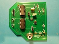
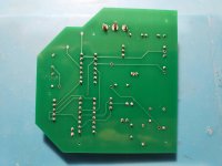
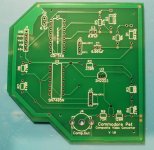
Here's the board, I included a shot of one of the non-populated boards' top side to be able to see the traces better.

20230211_071208.jpg
20230211_071242.jpg
20230211_071251.jpg


I'm pretty sure I don't have the transistor backwards but maybe I misread the datasheet?
 
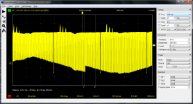
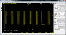
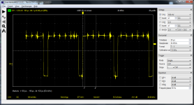
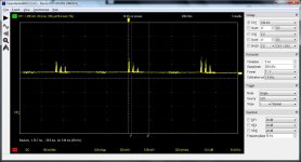
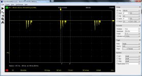
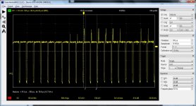
I'm not really sure what scale I should be looking at here with regard to either voltage or time but here's some captures of the composite output:

1676119139543.png

1676119193585.png

1676119266400.png
 
It looks like the sync pulses are there, but no video visible, that might be because there are few characters on the screen. The sync level is about right, for an unterminated condition at 544mV (exact would be 600mV), it should drop the 1/2 that level when terminated at the VDU end. In the meantime, just connect a 75R resistor on the pcb output to terminate it for testing. On your trace, both the H and V sync pulse look about right, despite that the VDU wasn't locking to them. The VDU you were feeding it to, does it have a 75 Ohm input resistance ? Your pcb may in fact be working. The H sync looks about the right width at around 5 or 6uS and the V sync width looks about right too at around 3x H periods wide.

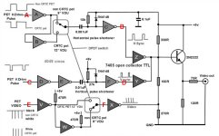
Ok, lets just check that the pcb is receiving the correct signals from the PET and the the pulse shorteners are working, before they are mixed at the output stage by the open collector gates. Fill the screen if you can with characters, so it will be easy to see video pulses.

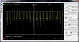
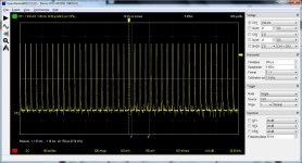
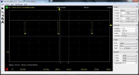
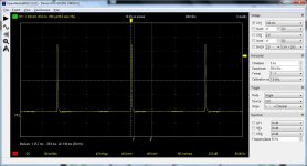
Can you take scope recordings of the six points A,B,C,D,E & F in the attached diagram. Keep the scope on DC coupling. Also mention where the zero volt line on the trace was before the scope got attached and set the scope to show at least 3 to 5 cycles of the pulses there. Then we do a final trace of the video output with it terminated into 75 Ohms. These recordings will confirm if it is all working normally, then if it is, we might have to work out why the VDU is not locking to it. Your VDU can definitely lock to a 20kHz horizontal rate ?
 

Attachments

  • test.jpg
    test.jpg
    115.3 KB · Views: 8
Last edited:
Okay will do! I'm heading out today with the wife but I should be able to do this tomorrow.
In post #346, which shows the VDU not in H lock, was it in V lock ? was there any vertical rolling of the image , or was that stable ?

The number of tilted line groups in the image suggests that the H osc in the VDU was running at a significantly lower frequency than 20kHz.

(One good thing about the circuit, it is dead easy to alter the sync pulse widths, if we ever have to, just by changing the two charging resistor values)
No vertical scrolling, I can get that going by tweaking the v.hold on the monitor but normally it seems stable vertically.
I do have a set of tiny variable resistors I can swap for these fixed ones to find the correct value. Probably R1 and R5 (the 0.01 and 0.001 ones?) I could start with setting the pots to those values and swap them in place of the current ones, then gradually adjust the values.

But for now I'll work on scoping the test points you mentioned, I should be able to do that in about an hour
 
Back
Top