• Please review our updated Terms and Rules here

Neglected PET needing some love

Voltage, speed, current consumption are factors.

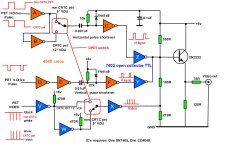
In this case, however, the key thing is that a 7405 is what is known as an open collector device - that is it only 'pulls-down' signals.

You will see that (in all cases bar one) that the red gates (CMOS) drive the blue gates (TTL open collector) - so the different parameters/functions of the gates come into play here.

There is one place where two red CMOS gates are in series with each other. I suspect this is for interfacing a PET logic signal to a CR (capacitor resistor) network for timing purposes. TTL have a wide range of parameters, and these could affect the required timing of the sync pulses.

Hugo will be able to add more information if course...

Dave
 
It is certainly my experience that the composite input on most standard definition TVs and monitors will be internally terminated with 75R so they need stronger drive than anything available from a typical logic IC output. Hugo's circuit in #319 has a suitably buffered output.
 
It may well still work of you leave out the two series 4049 gates ( but they would also be spare in the package) driving the timing capacitor with a TTL IC output from the V. drive pulse in the computer, is a little less predictable for the exact timing, or pulse width, because of the initial charge on the capacitor prior to the pulse start. The 4049 IC that drives the capacitor (to make the poor man's mono-stable circuit) has a symmetrical cmos output stage that swings close to rail to rail (unlike a standard TTL, but cmos is closer closer to TTL with a pullup). As Daver2 said, it is a timing thing.

With the cmos gate driving the capacitor, as they did it in the SOL-20, we can be 100% sure we get the correct width pulses. (Though as I mentioned they accidentally made the V sync pulse about 3 times too long in the SOL and used a 100k resistor, when it would have been better to be around 27k to 33k ). But the values they used in the SOL were about bang on for the H sync pulse width. At least with this circuit, if there is any issue with the sync pulse widths, they are easily adjusted with the resistor values.

Because I had not built this circuit yet myself, I tried to make everything as predictable as possible to avoid any problems.

The timing cycle for this type of monostable starts when the output of the first gate, driving the capacitor, falls low. Initially, at least some time after the previous timing event, the capacitor has close to zero volts on it terminals. When the output of the first gate driving the capacitor goes low, so does the input to the second gate. The output of that second gate goes high. The capacitor then starts charging via the resistor until the threshold voltage of the second gate is reached, which is around 1/2 of the power supply voltage for cmos or about 2.5v. At this point the output of the second gate falls low, that creates the shortened pulse. After a while, the output of the first gate goes high again corresponding to its input falling low, when that happens it would take the input of the second gate about 2.5V above the +5V rail because the capacitor was charged to about that value, but the diode conduction prevents that and the capacitor gets very quickly discharged, or "reset" because the output resistance of the cmos gate is relatively low. So the capacitor is then "prepared" with close to zero volts on its terminals for the next timing cycle. Some designers put a low value resistor like 47 to 100 Ohms resistor in series with the first cmos gate's output, to limit the current pulse, when the diode conducts and the capacitor discharges, which is reasonable, but many rely on the output stage in the IC to limit the capacitor's discharge current.
 
Last edited:
Okay I'll try playing around in a PCB cad program (that'll be a first for me) to get an idea of how things should lay out physically then try doing a prototype with some prototyping board. One thing I think rather than using a switch I'll use two sets of pin headers/jumpers as toggling between non-CRTC and CRTC isn't something one would be doing often.

One question, could the ground on the 0.1uF cap (upper/right) be shared with the grounds used around the composite output (lower/right) or should those two grounds be independent?
It is the same ground or common on the pcb. If you wanted you could also parallel a 10uF Tant capacitor with than 0.1uF cap, it could be helpful depending on how noisy the 5V supply is. The 0.1uF cap is really the minimum requirement for the two logic IC's . Some people use one 0.1uF capacitor for each logic IC's power supply.

It probably would make little practical difference, but my calculations on the base circuit of the 2N2222, suggests that the 100R resistor, would be better to be a 110R resistor, but it is such little difference, it hardly matters.
 
Last edited:
Damn I went looking for some CAD software, tried kicad but it wouldn't run on my windows 7 machine. I'm pretty hard set on not installing any version of windows above 7 and when I absolutely have to upgrade I'll probably go with some flavor of linux but don't really feel like doing that right now as there's still a few windows only games I like to play.

Anyway I looked around for some other cad software that was free and I've been working in one called "PCB Layout". After working with it for a few hours and actually making pretty good progress I had a little voice in my head that said "at some point you should make sure this will actually export to a format that I can send off to PCBway or some place else, like a gerber" and well... it doesn't. Actually the only export option is to "Order PCB from Bay Area Circuits" (which BTW would cost $75).

Then I went looking for other free/open source solutions and found one called FreePCB but it's kind of ... not very good.

I don't know either I'll keep hunting for a proper piece of CAD software or maybe divert my attention to installing a dual-boot win7/linux setup on my PC so I can run kicad under linux. Of course getting *anything* to run under linux, for me, has historically been a quest all on its own.

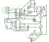
Anyway just for the hell of it I went ahead and finished up the design in PCB Layout because it's a fairly easy and intuitive program and I liked working in it even though I don't see any way to export it to anything useful. Here's what I came up with.

hugosDesignPcb_draft1.jpg
(note quite the right symbol for the RCA jack but best I could find)

For reference I added labels on the gates in your schematic, A-F for the ones in the SN7405 and V-Z for the ones in the CD4049.

hugo's design labeled.jpg
 
Divarin, I'm impressed that you didn't get caught out by the non-standard Vcc pin on the 4049 (also applies to the 4050 chip). I probably would have taken the +5V supply to pin 14 without a second thought. Of course, there's a reason why I am aware of this quirk, having been caught out by it at least once in the past...
 
Divarin, I'm impressed that you didn't get caught out by the non-standard Vcc pin on the 4049 (also applies to the 4050 chip). I probably would have taken the +5V supply to pin 14 without a second thought. Of course, there's a reason why I am aware of this quirk, having been caught out by it at least once in the past...

Hehe, this is one area where my lack of experience actually helped I guess. Although thinking back now I guess it does seem that the VCC is usually on the last pin but I didn't really think about it and I'm not experienced enough yet for that to be instinct that so I was just following the datasheet.
 
This is why (as you become more experienced) you start to make more mistakes (as you rely on flawed assumptions). As you become more experienced after that, you learn to check things rather than rely on flawed assumptions, and you make less errors...

Dave
 
There are some mix ups on the pcb labels, briefly it shows the H & V drive inputs connecting to what is labelled as the 7405, but of course those feed the 4049. If I just swap those IC labels though, then the IC's supply pins are wrong. And of course the 4049 is a 16 pin IC, not 14 pin, + power on pin 1 and gnd on pin 8. But the diagram shows two 14 pin IC's.

Yes, it pays to check for non standard supply pins on IC's, the other common garden non standard one is the 7493.

One other thing to consider, the 4000 series cmos were super fragile to electrostatic damage. The B suffix series better. But still, the input to a cmos gate simply looks electrically like a very small value capacitor and substrate protection diodes are not all that robust.

From the relation V= Q/C, with the capacitance C so small it doesn't take much electric charge Q to raise the input voltage V very high and destroy the gate. So adding some additional diode protection on input pins can help, if you make some module, where the input pins of cmos gates just go to a connector and the module can be sitting around unplugged on a bench sometime, and you walk over to it, get charged up, and pick up the board.

On the H drive and V drive cmos gate inputs, a 1N4148 diode to the + and - supply rails protects them well. Cathode of upper diode to +5V and anode of lower diode to ground. The diodes don't conduct in normal use, but will if the unit is unplugged and a bolus of charge comes along. One other option which helps a little if there are floating cmos inputs at times, on modules etc, is to use a tie resistor to ground of a high value to ground or+5 that won't interfere with any circuit driving the input, like 47k to 100k, or in this case it could be lower added as 4.7k to 10k pull up resistor to +5v, because the inputs are driven by TTL out of the PET (I think has pullups in the VDU). At least the resistor depletes any gate charge in the condition when the module is not plugged in.

So probably the simple thing is just add 4.7k or 10k pullup resistors to +5v on the inputs of the two 4049 gates fed by the H & V drive signals. I probably should have thought to put those two extra resistors on the diagram, because it also makes the cmos input more compatible with TTL outputs, in cases where there no existing pull-ups on the TTL output.

On the other hand, floating TTL inputs are relatively robust and can be left like that on some module that gets unplugged from time to time.

Also, on an actual pcb it pays to make all the ground tracks as wide as possible, don't scrimp on the copper in the ground tracks, but the more you leave the less is etched away.

There are lots of manufacturer variants of the 4049:

HEF4049 (Phillips), MC14049 (Motorola), CD4049 (Texas Instruments and National & RCA) etc. And they are available in plastic & ceramic packages.
 
Last edited:
On a related topic, the 2N2222 is a very historical transistor, which I have used over decades, cloned into many sub-standard plastic variants and re-labelled PN2222. I would avoid the plastic ones, I only use the original National metal can types with gold plated leads, like these:


or these:


Also Harris made a really very beautiful 4049, but they are more expensive than the common garden ones:

 
Last edited:
Oh man I can't believe I got those chips backwards, and that I didn't even notice the 4049 was a 16 pin chip. I'm still trying to learn this cad software, I wanted to place a copper pour around most of the perimeter as a ground plane but so far I'm not seeing how to make that actually connected to the ground pin, I'll figure it out though.
 
As ever, with any new piece of software, there is always a learning curve I am afraid.

I went through exactly the same learning curve with KiCAD...

Dave
 
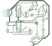
Okay I think this is correct now, swapped the chips around and made both the ground and voltage traces thicker. I also changed out the diodes with through-hole, didn't mean to use surface mount the first time.

I noticed in the schematic that the caps are non-polarized, but I have a huge bag full of polarized electrolytics (of various values) I was wondering if it should be safe to use those provided I have the polarities correct.

petCompV2.jpg
 
The 0.1 uF capacitor is a decoupling capacitor - so you really need a ceramic part for this role. Short bursts of high current for when the devices switch. These would be non-polarised.

The 0.01 uF and 0.001 uF capacitors are used to produce correctly-timed synchronisation pulses. The tolerance on electrolytic capacitors is abysmal (+/- 20% if you are lucky). The whole purpose of the front-end circuitry is to produce the correctly-timed synchronisation pulses so (in my opinion) this defeats the object of the exercise. I would use accurate capacitors designed for timing in these roles. These will also be non-polarised.

I would also be surprised if you could find electrolytic capacitors of this low value.

Dave
Oh okay. Thanks.
 
Best practice usually has the 0.1uF supply decoupling capacitors as close to the IC power pins as possible - on a large board the aim is usually one decoupling capacitor per IC with each capacitor typically placed at one end of its associated IC.

I wonder whether the video output buffer stage would appreciate a supply decoupling capacitor across its power rails as well?
A few examples:

for the 0.1uF capacitors, monolithic ceramic types work well, they come in blue and mustard color typically, these generally replace the larger sized ceramic disc types:


For the timing capacitors though, as noted these ceramic types are not ideal and better types are MKT film types that generally look like this:


or Wima make nice 5% ones, like this:


The best capacitors are Polystyrene types for timing applications, but they are not really necessary in this circuit and 10% MKT capacitors are ok .

On filtering the supply to the transistor, if the +5V supply is really noisy, a series resistor can be placed in the collector circuit, say 22 to 27 Ohms in this case. And a 0.1uF monolithic ceramic capacitor added from the collector to ground. This filters high frequency transients off the transistor's collector and it also shifts some of the transistor's heat dissipation away from the transistor junction and into the resistor because it lowers the average collector voltage due to the drop across the resistor. But the resistor cannot be too large in value, or it can result in the transistor's C-E voltage falling too low and the transistor saturating and failing to buffer. On the original design with 2N2222, they used a 47R resistor in the collector and no bypass capacitor. I simply left that resistor out and increased the transistor's emitter resistor instead, lowering the dissipation a little that way, it avoids an extra part. It is a fairly low power circuit.
 
Best practice usually has the 0.1uF supply decoupling capacitors as close to the IC power pins as possible - on a large board the aim is usually one decoupling capacitor per IC with each capacitor typically placed at one end of its associated IC.

I wonder whether the video output buffer stage would appreciate a supply decoupling capacitor across its power rails as well?

Hmm, okay. I can move C2 closer to U1 but how would it be connected electrically? Should one end of the cap be connected directly to the VCC of U1 and the other to the GND of U1?

Here's what I'm thinking:
v2v3compare.jpg

With the previous configuration on the left and the proposed new one on the right.
C2 (the 0.1uF cap) was moved near U1, the +5v connection is now connected directly to the input pin on J1 and the ground is connected to a pad which is then connected to the GND of U1 and the GND pin on J1. Also R2 was moved to the center of the board.
 
Back
Top