• Please review our updated Terms and Rules here

Original-IBM-5150 or IBM-Clone Memory Experimentation Thread

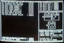
Sorry about the long wait. I had to wait for my diagnostic card to get in. I discovered something extremely odd. NOW the entire Supersoft Diagnostic runs, and it MAY be reading memory (not completely) somehow.

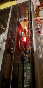
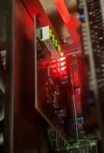
Anyways, I took out the two cards I had installed in the machine (A Western Digital 8/16 Ethernet Card and an XT-IDE CF card), and plugged in the diagnostics card. To my surprise, there was nothing frozen on the card's seven-segment LEDs. Even more strange, the screen now works properly, and it runs through the tests as normal. (Previously, with the diagnostic ROM, the picture would be unstable and roll, and it would stop at the Timer 1 test.)

I wonder if the previous cards had anything to do with it...
 

Attachments

  • 20210114_132342.jpg
    20210114_132342.jpg
    183.8 KB · Views: 3
  • 20210114_132358.jpg
    20210114_132358.jpg
    121.5 KB · Views: 3
  • 20210114_132301.jpg
    20210114_132301.jpg
    250.1 KB · Views: 3
Yeah, this is weird. It's as if the problem with my computer is not how the memory is connected, but failing chips (Some of which I did get from China). It is reporting errors on memory banks, but not all of them. Some seem to actually be succeeding!

Would a real IBM not run if any memory chips in the 16K area were faulty?
 
Last edited:
I've forgotten... I'm actually getting the same consistent bit pattern errors across at least the first 256K of the upgraded RAM, and it's always in consistent address increments.
e.g. 2000h, 4000h, C000h, 12000h, 14000h... (Yes, I know that this is not correctly incremented. I'm trying to prove a quick point.)
 
Been a while. I'm still trying to figure out this stuff, but I think I've found analogous chips between the 5160 schematic and the Sanyo. And as expected and what has been said before, there is one 5160 chip on the schematic that does not exist on the Sanyo, replaced by the mess of logic chips, that performs the same functions, that I'm trying to organize.

I've been routing logic lines all week, looking for similarities as well, between the Sanyo and schematic.

The one thing I'm having problems with is trying to route the RAM Address select line on the Sanyo map I've drawn up, so I can figure out where the logical clone of this "decoder" chip starts. (as I inaccurately called it earlier.)
 
I thought I had something, but it's turned weird now.

I've heard of a jumper being added to a location on the normal 5160 board to get 640k to work, and the only other jumper available that was near the memory logic was a unpopulated one. (and it seemed suspicious because there was a resistor connected to one via of the through-hole pair, with another resistor behind it and a trace snaking off somewhere on the board.) So I added a pin header and a jumper to it.

I'm still having problems, and the reason why I said it was weird is because I took bank-after-bank of memory out to make sure the Supersoft diagnostic would detect that some of it was missing, but it's now reporting the wrong kind of error, which is what it did before: a memory failure at address 05040, with the same failing bits in memory (7,6,1, 0, or so), even though none exists on the board now.
 
Last edited:
Okay, last post of today. I'm looking at other clone systems that used 640k of RAM to see if I have my ideas straight, and if there are similarities between them and the Sanyo.

Namely, I'm using this schematic from a Turbo XT computer: http://minuszerodegrees.net/manuals/...on%20Guide.pdf

So far, I've seen a lot of similarities. They both use 373s, 244s, and 245s in-line with the memory, for a start. However, they all use similar composite color output circuitry, too (Both with a "color adjust" variable capacitor, for one.)
 
I'm still having problems, and the reason why I said it was weird is because I took bank-after-bank of memory out to make sure the Supersoft diagnostic would detect that some of it was missing, but it's now reporting the wrong kind of error, which is what it did before: a memory failure at address 05040, with the same failing bits in memory (7,6,1, 0, or so), even though none exists on the board now.
Be wary of the Supersoft/Landmark diagnostic ROM. It is not comprehensive. I doubt that its RAM test is looking for addressing issues.

And the address of 05040 is a known red herring. Example at [here].
 
Last edited:
Would this be a better diagnostic to use, then? https://www.vcfed.org/forum/forum/ge...d-compatibles=
That is Ruud's diagnostic ROM. It is based on the Supersoft/Landmark diagnostic ROM. It is good for the scenario of '16KB-64KB version of IBM 5150 motherboard with RAM problems', because in that scenario, the Supersoft/Landmark diagnostic ROM presents misleading RAM failure information. See [here].

(EDIT: Never mind, it doesn't seem to be hosted anymore...)
Works for me (the link in the first sentence of post #1 of the thread that you pointed to).
 
It may be tentative, but I may have a lead.

Just from what I've seen in two schematics (IBM 5160 and Turbo XT Clone), the 158s are where they're supposed to be. They're all connected to their proper resistors.

But, looking over the board, I found something that seems off. In the two schematics, I've found that coming off of the Write Enable pin (Pin 3), there's a 30ohm resistor.


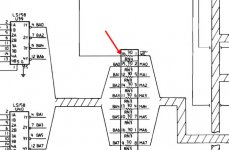
ibm 5160 sheet 6.jpg - Click image for larger version  Name:	ibm 5160 sheet 6.jpg Views:	0 Size:	61.6 KB ID:	1205241


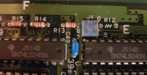
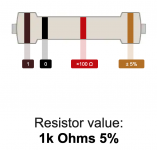
HOWEVER... connected to the write-enable pins of the memory sockets on the Sanyo is a resistor (R13), but it's a... 1kOHM?!

ibm 5160 sheet 6.jpg - Click image for larger version  Name:	ibm 5160 sheet 6.jpg Views:	0 Size:	61.6 KB ID:	1205241

ibm 5160 sheet 6.jpg - Click image for larger version  Name:	ibm 5160 sheet 6.jpg Views:	0 Size:	61.6 KB ID:	1205241

I looked through BOTH schematics and didn't see a 1kOhm resistor anywhere. I found 82k, 8.2k, 4.7k, 510, and 30ohm resistors, but never a 1kOhm...

Even worse, it seems to have NO continuity through it, as if it burned out or failed, but without any heat. (I had continuity through the other 30ohm resistors, and they were within spec.)

It's too early in the morning to do anything about it, but this seems like it doesn't fit in where it's supposed to be.
 
Last edited:
Ok, checking through the schematics one more time, I have a bit of a question...

Did the IBM PC use a voltage divider of two resistors to produce the logic levels for its read and write enable operations? Because according to a calcuator, I get:

Voltage Source: 5v
Resistor 1: 4.7 kOhms (In-line with a 243 output pin)
Resistor 2: 30 Ohms (in-line with the WE pin)
Output Voltage: 0.032v

BTW, on the second schematic (Turbo XT IBM clone), I found the same thing with resistor, except it was 33 Ohms.

But logic levels on a 4164/41256 seem to suggest that at least 2.4v is needed to drive the Write Enable Pin Active HIGH.

So then that means, on the Sanyo, with the voltage source coming from a 244's NOT gate:

Voltage Source: 5v
Resistor 1: 4.7 kOhms (on the 5v rail)
Resistor 2: 4.7 kOhms (on another part of the 5v rail)
Output Voltage: 2.5v

BTW, the original calculations I have with the 1kOhm resistor on the Sanyo are:

Voltage Source: 5v
Resistor 1: 4.7 kOhms (on the 5v rail)
Resistor 2: 1 kOhm (on another part of the 5v rail)
Output Voltage: 0.877v

This last calculation doesn't make sense, although I could be thinking of this wrong.
 
Last edited:
I kind of lost track at exactly what you've done to the original Sanyo circuitry, but the long and short of it reads to me like you didn't quite grasp what I was saying about how memory addresses translate into the RAS/CAS bank decoding (and what needs to change in that decoding circuitry when you substitute 4x larger chips into a bank) and are still just going by a "well, these schematics all use the same parts except (resistor value here is different than that), maybe I should change the resistor value..." approach.

I took a look at that generic XT schematic that you linked to, and here's the question about the Sanyo you need to ask: on sheet 7 of that XT schematic (page 31 of the PDF) there's an inset detail showing where the "RAM ADDR SEL" and "RAM SEL A/B" signals that feed into the 74138s on Sheet 3 that control the RAS/CAS generation come from. That inset "explains" how the the jumpers on the motherboard that select RAM configuration basically act as address inputs to a programmed 74S287 PROM chip that select between two different "programs" for reacting to the state of top four address lines, A16-A19. If your Sanyo doesn't have the equivalent of this circuit on it then you need to create it from whole cloth in order to use the denser chips.

(This is why earlier I was emphasizing why it might be instructive to compare the 5160 schematics to the 5150; the former uses a PROM for bank selection, very much like this clone, while the 5150 is hardwired to only take one kind of chip in all four banks on the motherboard, either 16k or 64k depending on the revision.)

Note that this circuitry isn't necessarily going to be a PROM, it could be a programmed PAL chip or even just discrete decoding with '138s/139s, but the takeaway is that unless you can find a thing that can react in two different ways to the state of A17, A18, and A19 (on a 256k-only machine you only care that both A18 and A19 are zero when enabling the onboard memory banks while a 640k machine needs to care not only if A19 is zero, IE, you're under the 512k mark, it also needs to enable onboard memory if A19 is one but A17 is zero, IE, the 512-640k page. And don't forget it needs to produce signals to control RAS/CAS appropriately for whichever mode it's in) you are boned and have to rebuild it somehow. Scrolling back I do see this from April 19th:

Been a while. I'm still trying to figure out this stuff, but I think I've found analogous chips between the 5160 schematic and the Sanyo. And as expected and what has been said before, there is one 5160 chip on the schematic that does not exist on the Sanyo, replaced by the mess of logic chips, that performs the same functions, that I'm trying to organize.

Is that one chip that doesn't exist and replaced by a mess of logic chips the PROM? Then I think the point is pretty much made, the Sanyo is closer to being a 5150 clone than a 5160 clone, and unless you've completely analyzed the decoder circuitry and proven otherwise it's highly improbable that it has "hidden" 640k support.

If you had complete accurate schematics someone might be able to suggest something, but lacking this you're just shotgunning in the dark.
 
There is a place for a third 158, and a place for a 139 (whose A, B, and Y pins are connected, at least to other chips, like flip-flops and AND gates, and not left floating), and I think the logic for A8 is there, just from the pin mapping I've done:

The way it goes from the CPU is the address lines are connected to the inputs of a 373 IC, whose outputs are then connected to that extra 158, then to Pin A8 of the memory, which is what I need.

Looking at the original 5150 schematic, that extra 158 does not exist, so it's more-or-less not a 5150.

As for the RAM RAS and CAS and addressing, I'll try to look into that.

The other problem, if you saw it, was that one of the resistors, the 1kOhm one, was seemingly burnt out. No continuity whatsoever.
 
Last edited:
There is a place for a third 158...

Okay, so: if you've definitively traced pin 1 on the chip sockets to a multiplexer output then that is indeed a legit sign that they at least *thought* of supporting the larger memory size. (Perhaps of note is the fact that it looks like on that XT clone schematic they *don't* waste a whole '158 for MA8 control, the insets on sheet 7 suggest they used different logic... perhaps also of note is the fact that sheet #3 doesn't show MA8 at all, suggesting the reason that the memory size selection stuff is relegated to bits of sheet 7 is this is a patch on an existing schematic originally designed just for 64k chips.) Follow pin 1 from that '158 and confirm it's common with pin 1 on the '158s on MA0-7. If *that's* true make sure there are no pull-up resistors connected that might be screwing things up. If that *all* checks out then, well, let's pretend it's good and move to the other part.

On the 5160 schematic there's a line to the '245 bidirectional buffer U9 pin 19, sheet 5 the IBM schematic calls RAMADDRSEL. (On your generic XT schematic this signal is on U13, sheet 3.) Your Sanyo undoubtedly has a similar buffer. Find out where that control line goes, it's the one that enables the CPU bus to be driven to or from the memory on the motherboard. On the 5160 schematic look at sheet 3; the line is driven through an LS00 (DMA-control-related reasons) by an output from the 24S10 PROM that has the programming to decide whether or not the planar RAM is enabled. That is a 4-bit PROM, of which three outputs are used, so... now follow the Q1 and Q2 outputs from that PROM. The schematic shows that they pass through a jumper block (That so far as I can tell exists as a fossilized remnant of support for 16k chips?) into the "A" and "B" inputs of '138s U42 and U56. This is how the CAS/RAS signals are switched to behave differently for the two chip types; the programming of the PROM, based on (I assume) the status of its A6/A7 inputs, toggles which CAS/RAS set is active for what memory area, and whether that area covers a 256k vs. 64k space.

(The Generic XT's circuitry is largely the same; its jumpering layout is a little uglier.)

Again, it's instructive to compare this to the 5150. If we trace that same RAMADDRSEL line on the 1984 schematics (64/256k system board) for the 5150 to sheet 3 of its schematic you'll see it terminates on U48, a 74LS138, that only has input lines connected to A18 and A19 so, again, its only choice is to enable the buffer when the board is in the bottom 256k of the address space. Likewise if you look at the inputs for U47 and U65 they're connected straight to A16 and A17 so there's no choice: each CAS/RAS pair covers a 64k area, no other options.

Now it's up to you to figure out if the Sanyo is *actually* hardwired as tight as the 5150. Follow the CAS/RAS lines back to where they come from (presumably also '138s) and figure out what their inputs are connected to. If they're straight through to A16 and A17 then it's hardwired for 64k no matter what A8 on the memory sockets does. If they are *not* then trace them back and find out if it's a PROM, a PAL, a bunch of random circuitry, *whatever*, that's connected to A16-A19 and has some kind of input for switching modes.

Just spitballing here, if this was a 5150 and you asked me to a way to hack it to 640k (and don't care about butchering it) I'd say try pulling the A/B pins on U47 and U65 out of their sockets, removing U48 entirely, running a few jumper wires, and programming a GAL with the following inputs:

A16-A19
ADDRSEL
DACK0BRD

These outputs:

MA8 (need to get this to pin1 on the DRAMs somehow, probably involves trace cuts)
CASRASDRVA and B (goes to A/B on U47 and U65)
RAMADDRSEL

And the appropriate memory map equations. "deadbug" the GAL somewhere, and, well, cross your fingers.

I have a suspicion the fix for the Sanyo will be about that extensive, but maybe they went the full mile building a full dual-mode decoder they never intended to use.
 
Last edited:
... so, just to note, I posted kind of a novel about how to get started on figuring out the RAS/CAS generation but apparently I edited it one too many times and now it's wedged in the forum's shiny new spam filter. Hopefully it'll show up eventually.
 
Okay, so: if you've definitively traced pin 1 on the chip sockets to a multiplexer output then that is indeed a legit sign that they at least *thought* of supporting the larger memory size. (Perhaps of note is the fact that it looks like on that XT clone schematic they *don't* waste a whole '158 for MA8 control, the insets on sheet 7 suggest they used different logic... perhaps also of note is the fact that sheet #3 doesn't show MA8 at all, suggesting the reason that the memory size selection stuff is relegated to bits of sheet 7 is this is a patch on an existing schematic originally designed just for 64k chips.) Follow pin 1 from that '158 and confirm it's common with pin 1 on the '158s on MA0-7.

I haven't found that A8 pin from the 158s yet. I should probably start there, but the connections on all 158s at least go to either a 373 latch, or a 244 line driver, so there seems to be at least an intention.

If *that's* true make sure there are no pull-up resistors connected that might be screwing things up. If that *all* checks out then, well, let's pretend it's good and move to the other part.

Well, that may be the 1K resistor that I found connected to the +5v line. (I'm assuming one connected to a power rail is a pull-up resistor, and one connected to ground is a pull-down resistor. I understand the concept behind both types. Pull up is for quick power draw at startup, and pull-down keeps a pin from changing states/floating.)

Just spitballing here, if this was a 5150 and you asked me to a way to hack it to 640k (and don't care about butchering it) I'd say try pulling the A/B pins on U47 and U65 out of their sockets, removing U48 entirely, running a few jumper wires, and programming a GAL with the following inputs:

Nah. I prefer upgrading to what any machine was made to do at its best, without breaking or too much modification. If I had a 64-256k machine, that's another story, but somehow I see this being able to take 640k, and I want to try it. (I think I have enough 4164 memory to replace all the banks if it doesn't work.)
 
Last edited:
I haven't found that A8 pin from the 158s yet. I should probably start there, but the connections on all 158s at least go to either a 373 latch, or a 244 line driver, so there seems to be at least an intention.

Well, definitely try to verify that there's connectivity between Pin 1 on at least half the DRAM banks and one of the outputs of that "extra" '158; if there isn't any then that '158 is for some other mysterious purpose and not there to multiplex A16 and A17 for optional 256kbit chips. (And, again, verify that pin 1 on that '158 is common with pin 1 of whatever two '158s multiplex MA0 through MA15. If it's not common with them then it's not controlled by the signal they use to know if they're in the CAS or RAS cycle so, likewise, that would be proof it's for something else.)

Again, you need to start checking out the RAS/CAS generation and see if *its* inputs are connected straight to the address bus or if there's some kind of abstraction. If the inputs are direct from a '244 or '373 then it's almost a 100% certainty that the RAM bank addressing is hardwired for 64k chips *only*.

Pull up is for quick power draw at startup

Well, it's a little more complicated than that.

1: You might use a pull-up for the same reason you use a pull down, IE, you want to tie off an unused input to ensure it stays in a predictable state. There are various black-magic analog reasons that I don't have sufficient education/experience to get into that might influence your choice here if it doesn't strictly "matter" what the state is as long as it's stable.
2: if you have a single output feeding a large number of inputs (large "fan-out") sometimes a pull-up/pull-down might help improve switching reliability. I vaguely recall you saying you found this resistor on the Write Enable signal feeding the DRAM banks, that's a possible theory as to why it was there.
3: if you're mixing CMOS and TTL logic pull up/pull downs might be needed because of the different high/low thresholds.
4: You have a circuit that's driven by components that have open-collector outputs. You're more likely to find open collectors in situations where you have to, say, drive a long cable, but they do show up in other places.
5: probably other reasons, but that's all I can think of offhand.
 
Well, definitely try to verify that there's connectivity between Pin 1 on at least half the DRAM banks and one of the outputs of that "extra" '158; if there isn't any then that '158 is for some other mysterious purpose and not there to multiplex A16 and A17 for optional 256kbit chips. (And, again, verify that pin 1 on that '158 is common with pin 1 of whatever two '158s multiplex MA0 through MA15. If it's not common with them then it's not controlled by the signal they use to know if they're in the CAS or RAS cycle so, likewise, that would be proof it's for something else.)

It does, according to my pin routing.

Pin 1 [A-8] on all of the ram banks passes through a 30ohm resistor, and then goes to 1Y of the extra 158 (I'm assuming 1Y is the output of 1A and 1B), so it seems there's at least SOMETHING there. (and according to the IBM 5160 schematics, that is exactly what is supposed to happen.) Also, Pin 1 of all the other two 158s IS common.

But there is still the A/B pin of the 157/158s that needs to be determined...

I'll look into the RAS/CAS generation tomorrow.
 
Last edited:
Back
Top