falter
Veteran Member
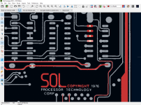
I've invested a bit of time trying to learn the ins and outs of KiCAD (it's the only software I'm even remotely familiar with for this task). I've been practicing on some Sphere boards as well as the Sol prototype PCB, trying to figure out which techniques work best for tracing. What I'm aiming for is very high fidelity to the layouts - keeping their 1970s 'handmade' styling intact. Upgrading to v7 with KiCAD was a huge help; it made bringing in an image file to trace a lot easier, and I've found a plugin that helps make curves. I set the grid to the smallest possible setting to allow fine adjustments to the traces.
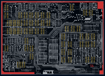
Where I'm a bit lost is things like IC pads - KiCAD as a bunch in its library but they're modern looking - I want them to look like in the first attached image. At first I tried making shapes, but then I couldn't put a thru-hole in the middle to connect to the other side. I then tried doing it with tracks, and I can plant a via in the middle but I'm not sure what that comes out looking like on the other side, or how the board house would interpret it.
It's been suggested to me to just treat the artwork as art, and simply import the cleaned up images I have from the construction guide. My concern with this is how to line them up properly, since they will definitely not be perfect for that, and then again how to handle vias, etc. There are also other oddball shapes, some are easy enough to draw out but again, how to put vias in them.
I note Labomb was able to come up with an amazingly accurate reproduction of the Sol prototype board, but I'm not sure exactly how he traced things so faithfully or what software was used.

")