• Please review our updated Terms and Rules here

TTL 74181 ALU, Need an ACCUMULATOR Register, Suggestions?

mmruzek

Experienced Member
Joined
Sep 28, 2011
Messages
229
Location
Michigan, USA
Hi, I am building a simple computer for fun that uses the 74181 Arithmetic Logic Units. These ALUs were the basis of some of the older vintage computer designs. I am trying to identify a Register part number to use for the Accumulator (ACC). A unique feature of the ACC is that it stores the ALU combinatorial result, but does not change output state until the negative clock transition. (The ALU result depends on the input from the registers.) I can find all sorts of registers that change output on the positive clock transition, but not on the negative. Am I missing something? If I can't find a register with this property, I will have to store the ALU result in a temporary location, and load it back to the register for the ALU to use. Thanks! Michael
 
You can use whatever register I guess. 74175 is four bits. DEC often use 7489 for the register file. 16 registers in one chip. Another option is the 74170/74670 which has separate read and write ports. Only four registers though. Whatever edge is used for storing can be handled by an external inverter. Positive edge is the most common.
 
You could always invert the clock signal...

Checkout the PDP-8 LD12 - this is an existing design for exactly what you are trying to do!

Dave
 
if this is a design you are doing (not an existing design) you should consider latching all registers and state changes on the positive clock edge.
Most of the synchronous logic components are pos. edge. You don't want inverters or gates in the clock path. (race condition)
Your registers should be edge triggered not transparent. The output will change after the clock but the input will already be latched.
The register then will contain the values before the clock edge.
This is what input hold and propagation delay are all about.
 
You don't want to store the data on the same edge as it changes you really want to wait a half cycle to let propagate and capture on the positive edge. You don't want to try to capture it on the same edge that it changes unless you use a delayed clock.
Think of it as like a bucket fire line. Data is passed on one half cycle and grabbed on the other other. Nothing works well if every one is grabbing at the same time. Half need to pass at the same time the other half is passing.
Dwight
 
I wonder how every FPGA manufacturer got this so wrong. They all do common single phase clock with edge triggered latches.

Please Google synchronous logic
 
I wonder how every FPGA manufacturer got this so wrong. They all do common single phase clock with edge triggered latches.

Please Google synchronous logic

What makes you think that? When I built the Baby Baby (Really SSEM)

https://hackaday.com/2016/01/06/babybaby-a-1948-computer-on-an-fpga/

I have multiple phase clocks and clock things on multiple clock edges. Of course this slows you down because you have to divide the master clock, but for many problems its fast enough so you don't care.
 
My recollection is that for the 74xxx systems, it was not uncommon to see a 74199 or 198 used as an ALU register. You get shifting capabilities out of it as well, which can be handy in an ALU. These ICs were not included in the move to LS logic and are 24-pin wide packages, so they're strictly period-correct.
 
If the logic was created with latches, they would have pos-edge and neg-edge clocked latches. You can not make functional logic with latches of all the same phase, unless you have no feedback. Sometimes, one can design multiple latches of the same phase clock in series but in these, they still need at least one of the opposite phase before there is feedback. This same phase latch is used to hold a value longer that might have a lot of logic. In these cases, there is a delayed clock. I doubt this type of design is ever used as the programmable part of a FPGA but may be used in RAM blocks within a FPGA.
Using edge clocked flops, it can be done. In a FPGA, the compiler you use, should understand the terms setup and hold time limitations.
When flops are made, even inside TTL ICs, they are usually made with two latches. The clocks are controlled so that on the specified D to Q, the input latch is guaranteed to be opaque when the output latch is made transparent. This is done by slightly distorting the threshold of the clocks into the latches. In CMOS designs for high speed computing, it is not uncommon to see both latch transparent when the clock goes high ( for pos-edge flop ). This type of design requires a minimum delay between flops. It makes for faster logic but requires more careful design.
When designing logic, one has to be careful to understand setup time and hold time limitations. For TTL, with just buffers, one has enough delay to use the same edge clocks with flops. One can do latch design as well but again, you still need to understand setup and hold times.
It is possible to make the same phase latch designs but that requires minimum delay and a very short clock pulse, not a typical symmetric 50/50 duty cycle clock.
Dwight
 
That was why a lot of people used the 2901 in the mid-70s. You got a 4-bit ALU, shifter, and dual-port register file all in one package.
 
That was why a lot of people used the 2901 in the mid-70s. You got a 4-bit ALU, shifter, and dual-port register file all in one package.

A right shift was more important than a left shift. One can always just add the same two numbers together to get a left shift. Being able to right shift by two bits was useful for doing square roots, along with a non-restoring division type operation. ( I'm not sure I got the term right but it is the type of division where the remainder could be positive or negative and required and additional operation to make the remainder positive at the end. )
Dwight
 
By the mid-70s, LSTTL was a reality and high-level integratio like the 2901 n became possible. The 74181/9341 dates from, what 1970? I recall the excitement of "a whole ALU on a chip" being reported in the press. Already, some were talking about a "CPU on a chip".

I think early 181 designs used the 74195 register, then the 198/99. The 198 allows for implementation of rotate (left and right) shifts as well.

Things were moving pretty fast back then. Recall that only a couple of years earlier, the best that could be had was a half-adder.
 
Thank you everyone for your ideas and comments! As suggested, I looked at the old newsletters from the UK ACC. There is a homebrew design using the 74181 ALU in Volume 3, Issue 4. There really was nothing special about the registers or clocking being used, which got me to wondering why I have seen so many homebrew designs feeding the ALU output directly back to the ACC register, even though the register's output is feeding the ALU for the calculation...

Then the other commenst about timing and race conditions made me realize that the reason this type of design probably works is because of the propagation delay in the ALU and buffer: which allows the ACC register to 'snatch' the ALU output before it changes as a result of loading new data! Sure enough, I tried it on my hardware and it works fine with a 74LS272 register. I have to admit I am kind of surpised it works, because I am actually using the 74F181 which is really fast (~10ns some conditions). I'm wondering if this explanation seems reasonable? Possibly there are opinions about going this route. :)

This project is part of my effort to eventually build a homebrew stack machine. The original design is in a whitepaper by Eckert. I have a webpage about it here:

http://www.mtmscientific.com/stack.html

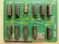
I've also attached an annotated photo of my ALU card. Thanks everyone for the comments. They really helped. Michael

alu_small.jpg
 
Many years ago for a digital design course final lab project I built a simple 8-bit CPU using 74LS181 ALU chips. I used AM2911 for the microprogram sequencers, maybe 3 of them for a 12-bit code address space. The 12-bit AM2910 sequencer might not have been one of the parts available to use, and AM2901 ALU parts must not have been available to use either.

The simple CPU was wired up to an original Mac mouse borrowed from a friend and a 6845 CRT controller to build a crude "Hack Paint". The CPU was just barely smart enough to be able to implement the Bresenham line drawing algorithm and not too much more. It was fun to get it all working at the time. One of the few things I wish I had kept from those days are the design files and final report I had to write up on that to remember how it all worked.
 
Back
Top