• Please review our updated Terms and Rules here

Vectrex (newer version - no buzz) - Troubleshooting Sound but no Video

Ah ha...

The change in Q503 collector corresponds to the brightness we see of the dot on the screen. This is good. I would have expected a greater voltage change myself - but the fact that we observe a change - and it is also being modulated with the Z-AXIS signal (this is - presumably - where the oscillating wave comes from) is very good. I can do a calculation later to verify what we are observing...

Q504 collector also has a healthy voltage swing now.

So the question now is why is the X and Y axis not deflecting correctly?

Back to checking the waveforms on both sides of R420 and R421 with your switch both OFF and ON.

In both cases you should have healthy deflection signals on Q401 and Q402 source leads.

Q401 and Q402 drain leads should be similar to the source leads when the switch is in one state, and much reduced with the switch in the other state.

If you don't get any joy on the drain leads of Q401 and Q402, it may be worth checking the signals on the gate leads.

Dave
 
Last edited:
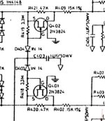
A negative gate voltage on Q401 and Q402 will turn the JFET OFF.

0V on the gate of Q401 and Q402 will turn the JFET ON.

Note that there is a resistor (R518) in series with the collector of Q504 (-19V to +5V swing) to the gate of Q401 and Q402 (also a diode) so the negative voltage swing on the gate of the transistors should be nowhere near -19V. Equally, the voltage shouldn't exceed +0.6V or so either.

Dave
 
Hi Dave. Looks like we are getting somewhere :) First of all, I am not familiar with this kind of Transistor. But I guess when you talk about the source leads you mean what is shown in the schematic as S and D, right? Gate is probably G and Drain is the leg to ground?

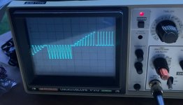
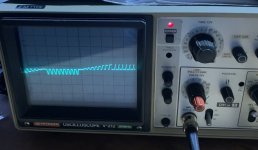
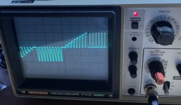
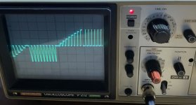
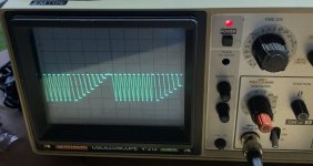
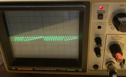
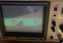
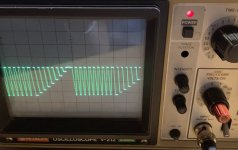
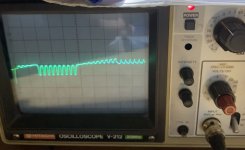
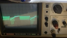
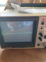
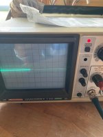
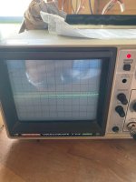
So, you are right I see good waveforms on both sides of R420 and R421. There is no big change when the switch is on or off. On the Drains of Q401 and Q402 I measure 0,00V

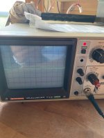
The Gates look almost healthy when the switch is on. When off there is static -18,7VDC on both transistors. When On I measure -220 mV on both. So, I am always below zero.

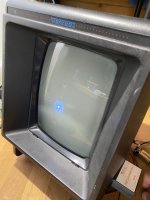
What is also interesting - today I found the spot extremely bright when the switch was on. So bright that I was concerned to burn my CRT. So I decreased the brightness a bit. I hope this is not influencing our troubleshooting measurements...
 

Attachments

  • Vectrex ultra bright dot.jpg
    Vectrex ultra bright dot.jpg
    2.5 MB · Views: 8
  • R421-Q402-D ON.jpg
    R421-Q402-D ON.jpg
    480.2 KB · Views: 6
  • R421-Q402-D OFF.jpg
    R421-Q402-D OFF.jpg
    464.8 KB · Views: 3
  • R421-Q402-S ON.jpg
    R421-Q402-S ON.jpg
    486.1 KB · Views: 2
  • R421-Q402-S OFF.jpg
    R421-Q402-S OFF.jpg
    476 KB · Views: 2
  • R420-Q401-D ON.jpg
    R420-Q401-D ON.jpg
    505.1 KB · Views: 2
  • R420-Q401-D OFF.jpg
    R420-Q401-D OFF.jpg
    528 KB · Views: 2
  • R420-Q401-S ON.jpg
    R420-Q401-S ON.jpg
    575.6 KB · Views: 2
  • R420-Q401-S OFF.jpg
    R420-Q401-S OFF.jpg
    594.7 KB · Views: 5
  • Q401 and Q402.jpg
    Q401 and Q402.jpg
    232.6 KB · Views: 8
uups. maximum 10 pictures allowed...
Here are the missing ones

Just realized that I forgot to check R518. Will do this next time.
 

Attachments

  • Q402-G ON.jpg
    Q402-G ON.jpg
    433.8 KB · Views: 2
  • Q401-G ON.jpg
    Q401-G ON.jpg
    449.9 KB · Views: 1
Last edited:
Ah ha, so now Q401 and Q402 are working fine!

Yes, D=Drain, S=Source and G=Gate. Not too difficult...

Decreasing the brightness to avoid drilling a hole in the screen (!) is good 👍.

I suspect now (if you look at Q503 collector) you will find a much larger voltage swing. Why, I don't know. But that would be consistent with the much brighter spot.

Ok, so a good healthy signal on Q401 and Q402 drains are good with the battery switched ON.

-220 mV on the gate is close enough to 0V (fully ON for the JFET transistors) as to not make much difference to the outcome.

The next port of call to measure with the oscilloscope is your favourite IC - IC401 pins 7 and 8 (inputs) and pins 5 and 10 (outputs).

Again, we are looking for a 'healthy' signal. The slight confusion may be the 'virtual earth' input on the inverting inputs of IC401. But we will worry about that later...

Dave
 
Good morning Dave,

Great. Thats good news.:) So seemingly all transistors are good (Q504 to be confirmed)?

Yes, the Voltage swing/amplitude at Q503-C is large at 17V (post #100). To see this I needed to adjust the V/div to the maximum of 5 and move the sweep all the way down.

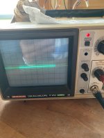
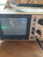
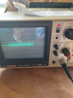
I did quick measurements at IC401 this morning before I went to my office. With the switch ON Pin 7 and 8 look a tiny bit better but still far away from a healthy signal. As yesterday my setting is 0,5V/div. Pin 5 and 10 look completely dead and slightly in the negative area. Should I see here a normal waveform like around the transistors?

Still need to check R518/Q504 but need more time to identify the resistor on the solder side.

Have a nice day, Dave :cool:
 

Attachments

  • IC401-10 OFF.jpg
    IC401-10 OFF.jpg
    577.1 KB · Views: 3
  • IC401-8 ON.jpg
    IC401-8 ON.jpg
    570.4 KB · Views: 2
  • IC401-8 OFF.jpg
    IC401-8 OFF.jpg
    558.3 KB · Views: 4
  • IC401-7 ON.jpg
    IC401-7 ON.jpg
    557.5 KB · Views: 4
  • IC401-7 OFF.jpg
    IC401-7 OFF.jpg
    571.7 KB · Views: 4
  • IC401-5 ON.jpg
    IC401-5 ON.jpg
    572.5 KB · Views: 3
  • IC401-5 OFF.jpg
    IC401-5 OFF.jpg
    567.3 KB · Views: 4
  • IC401-10 ON.jpg
    IC401-10 ON.jpg
    589.3 KB · Views: 4
You don't need to check R518/Q504. From your oscilloscope traces they are working fine also.

As I stated in my last post (with the beam being much brighter than previously) if you recheck Q503 collector I recon you will find a much higher voltage swing than circa. 17 Volts now.

I will think about how to test IC401 next... You never know, it might be faulty :)...

Dave
 
Last edited:
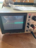
I think what you are observing on IC401 pins 7 and 8 is the 'virtual earth'.

This is where the voltage from Q402 drain (I will describe the Y-AXIS - but the X-AXIS is the same) is converted into a current by R409 (15k). There is an equal (and opposite) current fed back from the output of IC401 (pin 10) via R410. This makes the input (on pin 8) 0V - or at least close to it. This is why what your are observing with your oscilloscope is a very low voltage on IC401 pins 8 (and 7).

Look up operational amplifiers and virtual earth adders/summers for more information.

Let's take some preliminary readings first...

Measure the voltage on IC401 pin 1. This should be +9V (or fairly near).

Measure the voltage on IC401 pins 3, 4, 11 and 12. These should be -9V (or fairly near).

With the power OFF - measure the following resistors values:

R403 and R410 - 1M Ohm.

R407 and R414 - 3.3k Ohm.

R406 and R413 - 0.22 Ohm (a very low value)! Also, make sure that one end of each of R406 and R413 is securely connected to 0V/GND.

R405 and R412 - 1.5 Ohm (a very low value)!

Make sure C407 and C408 are NOT short circuit.

Let's see if that shakes anything out...

Dave
 
Hi Dave,

I don’t find the right voltages on the IC401:

Pin1: -235 mV
Pin 3, 4, 11 and 12: around -13,55 VDC

Something is wrong here. Some resistor values are far off and the capacitors C407 and C408 look suspicious. I hope I identified the right pins on the solder side but I could verify them when measuring continuity to their connections to the IC401 via R405 and R412. When measuring resistance across the pins I found both shorted. C407 with 2,7 Ohms and C408 with 4 Ohms. Normally when doing this these little capacitors are charged very quickly through the multimeter and the resistance goes up. Not on these ones. It is just strange that both look faulty. I also used my component tester to read the ESR but it only detects resistors with low Ohm values like I measured.

Here are my measurements about the resistors:
403 2,81 kOhm (right, no MegaOhm)
410 2,79 kOhm (right, no MegaOhm)
407 2,81 kOhm
414 2,78 kOhm
406 0,6 Ohm, connected to GND
413 0,9 Ohm, connected to GND
405 1,6 Ohm
412 1,7 Ohm
 
Question: are you measuring the voltages on IC401 with a multimeter set to Volts, and do you have the negative lead on the 0V/GND rail?

Dave
 
Just thought I would ask the dumb question first...

Can you measure the voltage across C109 and C117 please.

C109 should be -9V (relative to 0V/GND) and C117 should be +9V (relative to 0V/GND).

C109 should be 4,700 uF and C117 should be 10,000 uF.

IC401 pin 1 should be the +9V supply rail for the LM379 dual amplifier.

Measuring C407 and C408 is not as straightforward as I thought! There is a very low resistance path that (effectively) shorts out these capacitors... Anyhow - we are looking at voltages now around IC401...

Dave
 
Good morning Dave.

Not a dumb question. I understand why you asked. The funny thing is - this morning I measured stable +13V at IC401-1. Not sure why I got -0,2V yesterday. Maybe I made a short with my probes :confused: I always measure against the ground wire strap which connects both boards.

So, checked the capacitors 109 and 117. Measured both Pins against GND:
IC109: 0,00V and -13,5V - it´s a brand new 4700uF cap
IC117: 13,6V and 0,00V - it´s a brand new 10000uF cap

All good. I guess these numbers get closer to +9VDC and -9VDC when the Vectrex is running properly and pulling more current, right?

For properly testing C407 and C408 I obviously would need to de- solder them which is a pain as they are underneath the heat sink...
 
Ok, I probably wouldn't bother too much with C407 and C408 at this stage if it is difficult.

In order to duplicate our observed fault, both of them would have to be faulty in the same way - which is highly improbable (unless the same external failure compromised them both in the same way).

So, to confirm, we have the correct voltage power supplies on the pins of IC401. Yes?

Dave
 
Yes. Exactly. I can read them on all pins where they should be. Just a bit off +13V vs. +9V and -13,5 vs. -9V.
 
Good morning Dave.
So, maybe I should now go ahead and replace IC401? If this Chip is shorted internally it could also explain why it pulls down the deflection signals and also why I measure too low resistance across R403 and R410. Having the board on the bench I could also easily check C407 and C408 before pulling the chip.

Or is there something else I still can check?
 
I hoped we were on to something with the lack of the pin 1 voltage - but not to be...

It is less likely that it is going to be a passive component - because there would be two identical passive components (one in each channel) that would have to fail identically for us to get the same symptoms on both the X and Y. This is why I was looking for something that was common.

Now we have logically chased things through, the only likely active component candidate left is IC401.

It is a good little tool that we have developed in our Vectrex repair toolbox with the battery, resistor, diode and switch to manually enable the protection circuit. This has allowed us to chase things down to IC401.

I still think that the deflection input signals to IC401 will be close to 0V because of the virtual ground operation of the operational amplifier. I think this is a red herring myself; but we will see...

I have also found why R403 is not 1MOhm - it is in parallel with R407 (3.3k) that is in series with the deflection coils. This means you will measure less than 3.3k for the combined resistance (which you are).

There clearly is something wrong around here of course - hence we may as well replace IC401 at this point. It may fix your problem - but (equally) don't get too depressed if it doesn't.

Dave
 
Back
Top