• Please review our updated Terms and Rules here

8 bit IDE (XTA) Replacement Project

You are aware that an 8088/8086 bus cycle is four clock cycles...

I was aware that there was a 4 clock timing of the read/write operations although I thought it was based on a clock 4x the CPU clock. I must have misunderstood something when poking around on the Tandy 1000 board.

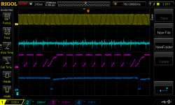
I wrote a little test program to do rapid register writes and explored a bit with the scope. I used a 486 DX2/66 with ISA clock set to 33/3. The chipset seems to drop this to 10Mhz by extending some of the cycles. I used this as I expect there will be 10MHz bus clocks on some of the 286 boxes. I have shared one image here, slightly more info is available at https://github.com/JayesonLS/8bit-ide-analysis

This image is shows about the first 1.5 IO write cycles of the ST05X BIOS code that does 6 rapid writes to port 320 to set the controller command registers. Yellow = CLK, cyan = XTA ~CS, magenta = D0, blue: ~IOW. The scope is not calculating the frequency of CLK well in this image - zooming out a bit seems to give a fairly consistent 10MHz. One interesting thing with the 486 is that the CS gets held low for long periods. I think the address lines do not always get updated on the ISA bus, which I guess makes sense since it is not possible to keep the slower ISA bus fully up to date with what is happening on the CPU bus. One thing I note is that the IO write (and presumably read) cycle seems to be even longer than 4 clocks. It does sound familiar to me that IO cycles are extended.

I also ran a routine that uses REPNZ OUTSB and the timing is identical on this 486. I think I am going to have to run these tests again on a 286 to see what happens. I do have a Tandy 1000 TL/2 which seems like a good fit other than the 8MHz CPU. Hopefully I will come across a 10MHz 286 XTA PC somewhere along the way.

Anyway, the data point I was after is that there is 13 clocks between each ~IOW. I was hoping it would be just a little longer but it think it work for what I have in mind. My hardware plan was to use at ATMEGA328 at 20MHz with an external universal shift register to hold the data. And a GAL22v10 to provide some glue. I like this approach as the bill of materials is inexpensive, can be all through hole and anyone with a TL866 can program the chips. Plus the timings on these micros is quite predictable.

The idea is that on an IO write, the GAL would latch the data into the shift register and signal the ATMEGA there was data. The ATMEGA would then trigger an SPI read. The SPI read would take 8 10MHz bus clocks to get the data out of the shift register, leaving at most 5 10Mhz clocks / 10 20Mhz clocks for the ATMEGA to detect the signal from the GAL and trigger the SPI read. I think it will just work. Especially if there is a requirement to use lower bus clocks if someone, for some reason, wanted to use an XTA card in a fast PC.

[EDIT] I set the 486's bus clock back to the default 8.33MHz. The period between ~IOW's is still 13 CLK's which gives an additional 5 20MHz clocks to the ATMEGA. I am excited - I think my plan is going to work.
Click image for larger version  Name:	NewFile2.png Views:	0 Size:	27.1 KB ID:	1224443
 
Last edited:
Good luck with this interesting project, I hope it'll be completed successfully.
Out of curiosity, does it cover a need/scenario were the XTIDE cards cannot be used? Or are you trying to provide an actual XTA drive replacement, even thought the XTIDE cards are an alternative?
 
Out of curiosity, does it cover a need/scenario were the XTIDE cards cannot be used? Or are you trying to provide an actual XTA drive replacement, even thought the XTIDE cards are an alternative?

I thought vwestlife made a important point in the linked video that XTA machines often have few or even no ISA slots. The early IBM PS/1 have no ISA slots and no XT-IDE type device. Tandy 1000 RL's only have 1 ISA slot. I think there are a few other machines with XTA connector but no ISA slots. Tandy 1100 maybe. I have a few projects I would like to work on and this one seemed most useful. A minimal sound blaster clone would be a lot of fun to develop also, but doesn't seem quite so useful. There are a bunch of sound card options, but there are zero XTA option as far as I know. Especially for the IBMs. Working Seagate 351 A/X's are not super uncommon, but working IBM drives for the Model 25, 30 or PS/1 don't seem to be very common.

There is a another point that is probably of less merit. You can get a little closer to the original experience with a solid state drive replacement. For sure, none of the glorious chirps that the WD steppers make. My XTA WD drive only works when it feels like it and when it does I am in early 90s heaven. One day it only worked once out of 20 boots, and when it finally did its thing, mmm-hm. This replacement would at least run the original bios. It is hard not to like all the color and options that XT-IDE offers but it does not feel period. I worked at a Tandy store (our Radio Shack) in the early 90's and I guess I have a desire to reproduce that to some level.

It is a weird thing that 30 year old electro-mechanical engineering is still far too advanced make reproductions of. I suppose that is a rabbit hole. Reproducing 60's silicon is bleeding edge amateur work right now.

I could have probably compressed all of that to: you can get solid state replacements for ATA, SCSI, MFM and floppy now, but not XTA. No ESDI either I suppose but I have no interest in that.

[EDIT]: I should probably note that at this point, it appears that IBM's 8 bit IDE used on the Model 25/30 and PS/1 is likely its own thing. I might have inadvertently signed up for two significant HD replacement projects.
 
Last edited:
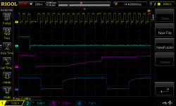
I ran my previous REPNZ OUTSB test on my Tandy 1000 TL/2 (8MHz 286). Scope capture below. The results are a little odd in that I never got a change on the IDE ~CS. Perhaps the TL/2 does not have it's XTA port at 320. Also, the time between ~IOW's is enormous compared to my 486 results. I expected it to be larger but this is crazy. I think I will just assume that the 286 timing is at least a bit longer than the 486 and move on.

NewFile1.png
 
I thought vwestlife made a important point in the linked video that XTA machines often have few or even no ISA slots. The early IBM PS/1 have no ISA slots and no XT-IDE type device. Tandy 1000 RL's only have 1 ISA slot. I think there are a few other machines with XTA connector but no ISA slots. Tandy 1100 maybe. I have a few projects I would like to work on and this one seemed most useful. A minimal sound blaster clone would be a lot of fun to develop also, but doesn't seem quite so useful. There are a bunch of sound card options, but there are zero XTA option as far as I know. Especially for the IBMs. Working Seagate 351 A/X's are not super uncommon, but working IBM drives for the Model 25, 30 or PS/1 don't seem to be very common.

There is a another point that is probably of less merit. You can get a little closer to the original experience with a solid state drive replacement. For sure, none of the glorious chirps that the WD steppers make. My XTA WD drive only works when it feels like it and when it does I am in early 90s heaven. One day it only worked once out of 20 boots, and when it finally did its thing, mmm-hm. This replacement would at least run the original bios. It is hard not to like all the color and options that XT-IDE offers but it does not feel period. I worked at a Tandy store (our Radio Shack) in the early 90's and I guess I have a desire to reproduce that to some level.

It is a weird thing that 30 year old electro-mechanical engineering is still far too advanced make reproductions of. I suppose that is a rabbit hole. Reproducing 60's silicon is bleeding edge amateur work right now.

I could have probably compressed all of that to: you can get solid state replacements for ATA, SCSI, MFM and floppy now, but not XTA. No ESDI either I suppose but I have no interest in that.

[EDIT]: I should probably note that at this point, it appears that IBM's 8 bit IDE used on the Model 25/30 and PS/1 is likely its own thing. I might have inadvertently signed up for two significant HD replacement projects.

Thank you for the detailed explanation, it makes much more sense now.
 
Anyway, the data point I was after is that there is 13 clocks between each ~IOW. I was hoping it would be just a little longer but it think it work for what I have in mind. My hardware plan was to use at ATMEGA328 at 20MHz with an external universal shift register to hold the data. And a GAL22v10 to provide some glue. I like this approach as the bill of materials is inexpensive, can be all through hole and anyone with a TL866 can program the chips. Plus the timings on these micros is quite predictable.

The idea is that on an IO write, the GAL would latch the data into the shift register and signal the ATMEGA there was data. The ATMEGA would then trigger an SPI read. The SPI read would take 8 10MHz bus clocks to get the data out of the shift register, leaving at most 5 10Mhz clocks / 10 20Mhz clocks for the ATMEGA to detect the signal from the GAL and trigger the SPI read. I think it will just work. Especially if there is a requirement to use lower bus clocks if someone, for some reason, wanted to use an XTA card in a fast PC.

Yay. I do know a *little* about the AVRs so maybe I could offer slightly more useful advice about those than ARMs.

Instead of using a shift register how about using a '573 parallel latch? If you use a contiguous port you can read a byte in a single instructions, access to the port registers is as fast as a memory read. The state machine you'll need to build into the GAL will be the same, IE, latch the data on a host WE signal and unlock it after the AVR signals a successful read. This will give you many more spare cycles to actually process the contents of a register write.

(FWIW, you might want to consider using the ATMEGA324 instead of the 328, because its larger number of I/O pins means it has several full 8-bit ports. From memory I think the '328 only has one? They cost about the same.)

Reads from the device feel like the trickier part to me:

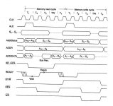
2332_8088%20timing%20system.jpg - Click image for larger version  Name:	2332_8088%20timing%20system.jpg Views:	0 Size:	52.7 KB ID:	1224484
The device we're emulating doesn't have just one register, it has four, selected by A0/A1. On either a read OR write cycle we'll want to grab the contents of those two address lines immediately as CS is asserted; for writes you could save that in another external latch and get it for later, but for reads you'll want to immediately use it (it's valid at the end of T1) to select the correct data value the host is asking for so you'll have it on the bus in time for the end of T3. This definitely feels like an argument for doing parallel I/O instead of a shift register.

If you really wanted to throw hardware at the problem here's a terrible idea: There's an old part called the 74670 which is a 4 bit by 4 address dual-ported register. A value can be written in one side at any time and read back out anytime on the other. If you used four of these, two for input and two for output, you could create a hardware-speed external register set that you could read and write basically completely asynchronously and timing almost wouldn't matter as long as you updated them once every 4x cycles. Keep the GAL and use that as a status register/interrupt generator state machine for the AVR so you can signal to it when a host access has happened. And, well, you're also probably going to have to implement a state machine for DMA data transfers, but maybe that's getting ahead of ourselves.

(* Edit: Or instead of a pile of '670s another idea might be a dual-ported memory chip. Renesas makes several models, they're kind of expensive but they could do the same job and more. If you had a 1Kx8 chip you could use 512 bytes of it as an input/output buffer for DMA sector transfers and 8 bytes of what's left for the I/O registers...

Another nice part about using the memory chip or registers to completely isolate the AVR from the bus is you won't need an external tri-state buffer.)
 
Last edited:
I ran my previous REPNZ OUTSB test on my Tandy 1000 TL/2 (8MHz 286). Scope capture below. The results are a little odd in that I never got a change on the IDE ~CS. Perhaps the TL/2 does not have it's XTA port at 320. Also, the time between ~IOW's is enormous compared to my 486 results. I expected it to be larger but this is crazy. I think I will just assume that the 286 timing is at least a bit longer than the 486 and move on

Did the TL/2 have a drive installed in it? According to this Tandy omnibus the 1000s with XTA ports do have them at 0x320. I wonder if the circuitry driving CS disables itself if it doesn't detect an XTA drive present. (Is that what the "ACTIVE" line on the bus is for? I can't find docs for that.) That would be a useful feature if a user installed a conventional HD controller instead.

As for the spaces between the IOW's, how is your test code generating the writes? This fastest way to transfer "arbitrary" data to I/O port on the 80186 and higher are the INS and OUTS instructions, which directly auto-increment from a starting address in RAM and push/fill RAM without the need of any LOOPs. A quick skim of the 286 reference manual says an OUTS takes 5 instruction cycles per REP, I'm not sure how that matches up with *bus* cycles on the 286 when it's doing 8-bit I/O with wait states, but in any case I think it's reasonable to expect that a 286 is likely to take "more" time than a 486. (The instruction timing counts in the 486 manual I simply have no idea how to interpret, but the 486 executes most non-I/O instructions *much* faster than the 286, which isn't even close to an instruction-per-clock for almost anything. And an XT is going to be even slower.) If you're just doing a series of non-string OUT without a loop, literally just directly transferring an already loaded register, then that probably would be the very fastest way to trigger IOW, but it's not exactly a "real world" case...

But, really, the timing that matters most is if I'm reading the 486 trace correctly you have 600ns between chip select and the end of the I/O cycle. If the plan is to fire an interrupt on CS the stated interrupt latency for the AVR appears to be 4 clock cycles after finishing whatever instruction is in flight. At 20mhz on the AVR that's going to be cutting it pretty close for reads, since you're going to have a minimum of 200ns latency and worst case... quite a lot if you were in the middle of something expensive and it has finish before responding to the int. If it could *always* just be 200ns you'd probably be okay since 400ns will give you 8 cycles to read A0/A1 to turn into an offset and read/write to see what the op is and read/assert accordingly, but the possibility that you could be neck-deep in something expensive when the interrupt fires complicates things.

This is where the harebrained idea of an external memory device to serve as the host-accessible read register might make sense. (Another idea for that is if the dual-port chip is too expensive you could make one yourself from a normal SRAM and some buffer/multiplexers since it strictly isn't necessary for it to be dual ported as long as you make sure you don't access it from the AVR during host cycles.)
 
This is where the harebrained idea of an external memory device to serve as the host-accessible read register might make sense. (Another idea for that is if the dual-port chip is too expensive you could make one yourself from a normal SRAM and some buffer/multiplexers since it strictly isn't necessary for it to be dual ported as long as you make sure you don't access it from the AVR during host cycles.)

Yet another option, albeit not necessarily a prettier one, would be to assign each of the four XTA registers to its own 8-bit output port of a sufficiently big µC and to interface them to the bus using four 8-bit tri-state buffers.
 
Yet another option, albeit not necessarily a prettier one, would be to assign each of the four XTA registers to its own 8-bit output port of a sufficiently big µC and to interface them to the bus using four 8-bit tri-state buffers.

It's a shame the '670 is kind of an abandoned part because a dual-port register like it is actually really useful. A bigger/wider one would be even better, but I guess at a certain point you're splitting hairs about whether it's just a dual-port RAM.

The datasheet for the WD11C00-17, which is the bus interface portion of the WD1002 controller linked earlier, is interesting reading. FWIW, and this is oversimplifying a lot, it is a state machine that has roughly the equivalent of several 74670's built into it for the status registers, a read/write buffer, and control lines to run 1K's worth of static RAM used for sector buffers and caching ECC data and commands for the controller's processor. (The part where it appears to be smart enough to cache full multi-byte commands for the CPU is certainly interesting.) There's a block diagram on page 1-3 of the WD1002 manual that's kind of useful for visualizing the task at hand. My broad-stroke take on it is an AVR 8-bit CPU should be more than enough to do the job of the WD1015 and *parts* of the WD11C00-17 (you definitely don't need ECC generation anyway, and it's probably fine doing its own command serialization...). The SD card has no need for and otherwise does the job of the WD1010A disk controller and WD10C20 data separator components, so they're out . But because the AVR simply is not designed to be directly slaved to a bus (no built in tri-state or external port R/W direction control, nor a way to "DMA" based on an address input) the task would get a lot easier if you had help in the form of external memory buffering and a little clever state-machine-ing. It's all about latency. If the bus had a WAIT line on it you could pull with the GAL on every I/O operation then, yeah, don't need it, but lacking that makes external memory a *really* attractive workaround in my mind.
 
You may want to consider using a PIC32MX MCU (based on the MIPS R4000 architecture). In particular, have a look at section 13.4 here

... the really juicy part seems to be section 13.4.3, "Addressable Buffered Parallel Slave Port Mode". In essence this mode looks like it's pretty much exactly what you'd get if you went with that idea of using four '670's and a state machine that'd let the processor know that a read or write happened. For some applications that it's limited to four addresses might be a bummer, but considering that's just what's needed here this actually might be the perfect solution.

I've never programmed for PIC before but I'm really tempted to look into this because a project that's been gnawing on me is a floppy disk replacement that targets emulating the whole shebang at the controller level. It just so happens a Western Digital 177x-type controller has four registers as well...
 
The PIC32 stuff isn't bad and the documentation isn't nearly as cryptic as the upper STM32F4 and F7 parts. If you want to program assembly, the instruction set is well-documented and not as involved as, say, ARM. The toolset is pretty good.

I got my first whiff of it with the Digilent Uno32--board--basically a souped-up Arduino.

I mostly use STM32 stuff now because it's more widespread, but the PIC32 isn't bad at all.
 
You may want to consider using a PIC32MX MCU (based on the MIPS R4000 architecture). In particular, have a look at section 13.4 here

This was looking just perfect. All the needed registers in a 28 pin through hole device that costs about the same as an ATMEGA328. Things might get a little tight on pin count but I reckon it would work. Unfortunately it is a not a 5v device and while a few pins are 5v tolerant, most are not. At least not on the 28 pin part. Level shifting always seems like a pain in through hole designs. Maybe a couple of 74LVC245A's would do the trick. This might still be the way to go.

A 5v micro with a single register and better than 80's performance would also be a good option. Only port 320 is full 8 bit IO register. From what I can gather, it reads/writes directly to the controller sector buffer SRAM and the SRAM address auto-increments. As long as the micro/register setup can keep up with the data coming in/out, all is good.

For writes to the other 3 ports: Two just signal when they are written to (reset and request-start-of-command) and have no data. The last just has two bits to enable/disable DMA and IRQ. I think all of this would fit into the proposed GAL22V10.

For reads from the other 3 ports: One is not used at all. One has 6 bits of status flags. One has 4 bits of drive size information. It should really only be 2 bits of drive info - the other 2 bits are for the second MFM drive which is impossible with XTA. A second drive in XTA presents as a second interface. However the two Seagate drives I have tested report their size info on both sets of bits. I suppose I should duplicate that behaviour just in case there is some BIOS somewhere that counts on it. These reads would not also fit into the one proposed GAL. I think an extra IC of some kind would be enough to take enough pressure off of the GAL. A register, tri-state buffer or maybe just a second GAL.
 
Did the TL/2 have a drive installed in it? According to this Tandy omnibus the 1000s with XTA ports do have them at 0x320. I wonder if the circuitry driving CS disables itself if it doesn't detect an XTA drive present. (Is that what the "ACTIVE" line on the bus is for? I can't find docs for that.) That would be a useful feature if a user installed a conventional HD controller instead.

There was something funny going on when I captured from the TL/2. None of the numbers make much sense so I am going to ignore the results until/unless I figure out what was going on. This test was using REPNZ OUTSB. I have a 1000 TX I can put the Seagate XTA card into and I'll see what I get there.
 
You can always go to the QFP packages. There are cheap adapters--I may even have few extra. Perfect for prototyping. A couple of years ago (well more, actually) I was working with the PIC32MX795 and still have a number of adapters unused (and am not likely to use). You populate them with a few capacitors and solder on the QFP and you're good to go. There's even a programming header for a PICKit programmer. Let me know.

There's also the more recent PIC32MZ line--still has the master port and 5V tolerant I/O (can sink up to 32 ma per pin).

Nowadays, it's STM32 for me, but that's mostly due to price and availability.
 
Last edited:
Instead of using a shift register how about using a '573 parallel latch?

That is definitely an option. The early Sound Blasters use something similar - a pair of 374's (one for each direction) and a 40 pin micro. I was looking for a bidirectional register to reduce chip count and could not find one. I did come across at least one suitable shift register though and that would make it easier to use a micro with less pins. I thought the FreHD for the Tandy Model 3/4 was doing something like this, but it is not - it uses a one-way shift register for reads. For writes and read setup time, it halts the Model 3/4 CPU.

(FWIW, you might want to consider using the ATMEGA324 instead of the 328, because its larger number of I/O pins means it has several full 8-bit ports. From memory I think the '328 only has one? They cost about the same.)
This does seem like a great option for a 5v, 40 pin micro. It is a little more costly than a 328, but not much so.

If you really wanted to throw hardware at the problem here's a terrible idea: There's an old part called the 74670 which is a 4 bit by 4 address dual-ported register.
I have a sleeve of these - I was thinking of designing a DMA circuit for old Tandy's.

I think for this project, if we are adding that much external memory, it is time to bite the bullet and use a CPLD.

And, well, you're also probably going to have to implement a state machine for DMA data transfers, but maybe that's getting ahead of ourselves.
Yeah, there are a lot of parts to implement.
 
The problem with CPLDs on old-school hardware is that there are very few 5V CPLDs--there are some with 5V tolerant inputs, but the only true 5V one that I know of is the Atmel ATF1504AS, but I don't know if Microchip is just shipping old stock.

Gone are the days of my favorites the Xilinx XC95 devices in PLCC fully 5V compatible.

Yeah. If PLCC XC9572 was still a thing, I would probably just drop one of those and an AVR on a board and move on. You can still source them - they are used in the CocoSDC. I think Ed Snider gets them from UTSource. Who knows for how long though.

I guess the ATF150x might not be a bad choice. And if it disappears, then switch the design to a pile of GALs. :) And if Microchip stops making those, used GALs are currently plentiful. I think the more general problem is that any 5v through hole friendly part has some risk of disappearing.

Actually, a board with an ATF1508 and a micro might be just the thing for development. Then optimize part selection later. I am not sure at all right now how to wire everything up and I am not a big fan of soldering a lot of wires during prototyping. The only thing giving me pause is imagining all the wincupl bugs I might run into. I am not clear on how to program it either.
 
Back
Top