• Please review our updated Terms and Rules here

8 bit IDE (XTA) Replacement Project

Umm, wow! Nice drive collection. Those WD's sound just wonderful in my opinion. When mine feels like working it is a happy day. I understand the desire to be able to use them.

Going the opposite way... could it be possible to add support for 8-bit IDE-XT drives to a modern XT-IDE interface card? The IDE-XT interface cards, like the Western Digital WD-XT150 shown below, are all very simple, with just a few off-the-shelf 74LS-series chips and a ROM.
[/IMG2]

I think Eudimorphodon is right that it would probably best to design a new card to make use of an original BIOS. It is not a complicated board. I expect you could actually run the WD BIOS on the Seagate card and vice versa. I was thinking I would design a card after the drive replacement was done. I thought some folks might want to be able to run a period bios. I kind of want to put one together right now. It would not take very long to do the schematic. I keep getting more pedantic in my board layouts with each new one I do, and so there is probably a solid couple of days of layout work to do.

I do have my XT-IDE CF variant to start with: https://github.com/JayesonLS/ISA-Cards#cf-combo-super-lite-1-2
 
xt140&xt150.pdf.jpg

Would it be possible to get a BIOS dump from this card? It would be very helpful. I have attached a text file which will dump out the entire BIOS range when directed into debug. If you zip up all the resulting ROM*.BIN files, I will be able to extract out the WD BIOS.

Code:
 debug < dumpbios.txt

View attachment dumpbios.txt
 

that's a beautiful sight, I had one of those drives as a kid and inserted the power connector the wrong way round - never did forgive myself for that

in my defense the thing offered basically zero resistance to the physical insertion and it had +5 on the right which is the opposite of everything else ever
 
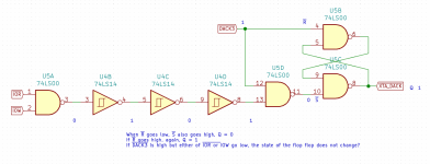
I could not help myself and started on an XTA interface card design. It was all going fine until I found this extra circuitry on the Seagate ST05X card for ~DACK. I must be misunderstanding something because it seems to do nothing. Can someone assist? The blue text is notes I added while trying to make sense of it.


Click image for larger version  Name:	huh.png Views:	0 Size:	288.9 KB ID:	1224681
 
Last edited:
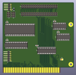
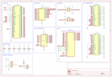
I am not sure at this point whether this is actually something useful, but this is current WIP on an XTA interface card.

XTA-Card-WIP.png

XTA Card WIP Schematic.PNG
 
I could not help myself and started on an XTA interface card design. It was all going fine until I found this extra circuitry on the Seagate ST05X card for ~DACK. I must be misunderstanding something because it seems to do nothing. Can someone assist? The blue text is notes I added while trying to make sense of it.

I think I would have to sit down and write out a truth table for the whole thing. Is it there to make sure DACK is de-asserted when a read/write cycle starts (ior/iow goes low)? It kind of stinks of a hack they might have thrown on there to deal with a known implementation bug with particular motherboards or drives.
 
Attached is a dump of the Seagate ST-05X XTA interface card BIOS.
 

Attachments

  • ST05XBIO.ZIP
    3.6 KB · Views: 4
I think I would have to sit down and write out a truth table for the whole thing. Is it there to make sure DACK is de-asserted when a read/write cycle starts (ior/iow goes low)? It kind of stinks of a hack they might have thrown on there to deal with a known implementation bug with particular motherboards or drives.

I plugged it into an online simulator and it does do something. It will hold ~DACK low while either ~IOR or ~IOW are low. I will implement it on my board.
 
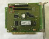
Does anyone have an ST05X card with the resistor(s) populated on the area I have highlighted below? It is not populated on my card and would like to know the resistor value. The HD activity LEDs are driven directly by the hard drive and the current capability is not documented. I'd like to keep things simple and just use Seagate's original value.

I know there is at least one person who would like to populate the resistor / LED header on their card also.

ST04X-LED-Resistor-Highlighted.png
 
I plugged it into an online simulator and it does do something. It will hold ~DACK low while either ~IOR or ~IOW are low. I will implement it on my board.

Looking at ISA timing diagrams DACK is supposed to be low until the end of IOR or IOW already. Again I suspect this is a fix for some common(?) bus timing mal-implementation discovered after the drives were built assuming everybody did it right. It’s a shame you probably have no chance of finding out why it’s there without tracking down an elderly Seagate engineer.
 
Looking at ISA timing diagrams DACK is supposed to be low until the end of IOR or IOW already. Again I suspect this is a fix for some common(?) bus timing mal-implementation discovered after the drives were built assuming everybody did it right. It’s a shame you probably have no chance of finding out why it’s there without tracking down an elderly Seagate engineer.

Yeah, and the timing diagrams I am looking at (http://www.ee.nmt.edu/~rison/ee352_spr12/PC104timing.pdf) show that DACK should be held for even longer than this circuit is doing. I am tempted to just remove it, but there must have been some reason Seagate decided to implement it. It is very annoyingly messing up my minimal 3 chip design :)
 
Here is the WD BIOS from my CompuAdd 810 motherboard, which has XTA integrated.


Thanks for this. I spent some time disassembling it with Ghidra and added it to the analysis project here: https://github.com/JayesonLS/8bit-ide-analysis

I learned some interesting things:

1. The BIOS determines the interface address based on the BIOS address. If the BIOS is at C800, the ports start at 320, otherwise they start at 322. I think to support two drives, it would require two copies of the BIOS. This would be the case if two WDXT-150's were installed. Both the BIOS address and the port address jumper on the WDXT-150 (W1 and W2) would need to be changed together.
2. The WDXT-150 has an IRQ 5/2 selection jumper. However, the BIOS reads the configuration from the drive. WD drives have jumper to make this selection. With Seagate drives, I think you would be stuck on IRQ 5. Quite strange.
3. XTA drives only have 2 drive size bits (4 possible sizes). The WD BIOS supports a second set of drive parameters for 8 possible configurations. Which set to use is queried from the drive - I think it might be the "physical/logical" jumper on the WD drives that changes this.
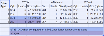
4. The drive parameter tables vary when compared to the ST05X bios. I think this is why the ST351 A/X has so many jumper configurations - so it can be fully compatible with Seagate and WD BIOS'es. Drive info below for future reference.

Drive configs.PNG
 
Honestly all this weirdness and kneecapping limitations seems to make a pretty ironclad case that the one practical application for an XTA replacement drive is machines that are stuck with XTA ports on the motherboard and no option to use an XTIDE or XT-CF with none of these problems, but I guess it’s useful to at least get all this documentation reconstructed.
 
Honestly all this weirdness and kneecapping limitations seems to make a pretty ironclad case that the one practical application for an XTA replacement drive is machines that are stuck with XTA ports on the motherboard and no option to use an XTIDE or XT-CF with none of these problems, but I guess it’s useful to at least get all this documentation reconstructed.

LOL. What, you don't want a hard to configure device that costs more than an XT-IDE lite, only gives you 40MB of storage and you can't easily pop the card in and out of the rear slot? But then you wouldn't need to also buy a controller card that costs as much as an XT-IDE lite.

Maybe I should have done a RAM + XT-IDE upgrade for the 5140 instead. :)
 
Maybe I should have done a RAM + XT-IDE upgrade for the 5140 instead. :)

Heh. I actually have that in my project queue, currently stalled for several reasons including the complete and utter unobtanium status of the rear bus connector. (The workaround I started going down is sacrificing the guts of a parallel/serial module instead, that’s “only” going to require laying out a card edge with completely proprietary spacing and severe space limitations.) Trust me, that thing is a heaping bucket of pure hurt. IBM actively went to great lengths to make that critter difficult for third party expansion. Even the internal RAM cards have a proprietary demux bus decoder on them. Every card does.
 
Heh. I actually have that in my project queue, currently stalled for several reasons including the complete and utter unobtanium status of the rear bus connector. (The workaround I started going down is sacrificing the guts of a parallel/serial module instead, that’s “only” going to require laying out a card edge with completely proprietary spacing and severe space limitations.) Trust me, that thing is a heaping bucket of pure hurt. IBM actively went to great lengths to make that critter difficult for third party expansion. Even the internal RAM cards have a proprietary demux bus decoder on them. Every card does.

I was thinking a double-size RAM card that added up to 512 of RAM, with 128K of that potentially being UMB, and JRide style memory mapped XT-IDE. You can't get the CF card out easily, but if you have the serial adapter (I do, so I guess I am biased), you can transfer files over that pretty easily. I am wondering now if maybe all the needed address lines are not available.
 
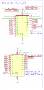
Getting back on topic, I think I will try to finish out the XTA interface card since I have put some thought into it. Plan is to make it configurable as either an ST05X, or a WDXT-150 card. I am going to use a pair of GAL16V8s for all of the glue logic. Keeps the part count down, and the BOM short. Also the least expensive option as far as purchasing parts go - Atmel's 16V8's are about 1.5x the cost of a typical LS logic chip and in this case, do a lot more work. The two 16v8's have a little logic to spare if future feature needs come up.

XTA decode.PNG
 
Back
Top