• Please review our updated Terms and Rules here

Cbm 2001 Pet strange boot

Happy for you to continue...
It's OK ;)

As part of my continuing documentation effort I attach the address bus traces you would expect when NOPing on a PET 2001 (similar to 2001N)... I've been meaning to get around to this for ages.
 

Attachments

  • PET Scope Traces - Address Bus.pdf
    120.7 KB · Views: 12
Nice document.

Is it worth adding a sample output signal from (say) /SELF to it? That would be a great document to add to a 'sticky' post...

Dave
 
Hi Dave please what can i do now?? I am desperate!!!

Nivag has already posted the two (2) documents you need initially. See the documents attached to posts #1,781 and #1,765. These are duplicating some of the testing that we have already done - but it is best to repeat it as I am now confused.

The first document (latest post) #1,781 shows perfectly how to capture the buffered address lines when the NOP generator is installed.

The second document (earlier post) #1,765 shows perfectly how to capture the /SELn lines for the RAM, I/O, ROM etc.

The particular chip references themselves may be different between your PET and Nivag's. The /SELn signals for your machine are from the outputs of the SN74154 at UD2.

Since you have successfully managed to perform some of these tests already - you should be able to duplicate the results that (a) Nivag has got and (b) that you obtained previously - albeit Nivag has a more comprehensive oscilloscope.

We can then start to look for the small pulses again when you have mastered these tests - although I think I have worked out why you may not be seeing the detailed pulses on your oscilloscope. If this is the case, we will have to rethink the trigger.

Dave
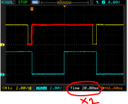
Please Dave, can we check for these pulses please? I already checked the other signals :(((((((((((
 
What happens if you use UD9/20 as the signal for channel 2 (set to DC) and used as the timebase trigger. Set the timebase to 10 ms/div and the trigger edge to (-).

Leave channel 1 on GND for the time being.

Adjust the trigger level until you get a stable trace.

Let's start with this first shall we. What do you observe?

Dave
Correct??

 
That looks about right.

Now, turn the timebase knob clockwise and see what happens as you turn. The amount of time that the wave appears at the bottom of the screen should increase. Keep turning the knob clockwise until you get to 1 us/div.

I am hoping some smaller pulses will come into view.

These pulses should have an amplitude of between 4 and 5 Volts.

I am not sure why the image doesn’t start fully on the left-hand-side though (unless you have the X-SHIFT / X-POSITION) adjusted incorrectly.

Dave
 
The trace in #1789 looks correct. It shows a short low followed by a long high. This is consistent with nSELF which has 8.2ms of LOW in the A15 period which is 131.2ms. It is left justified because it is triggering on the -ve edge.

At 10ms/div that makes the width of a low about 4 ticks worth (there are 5 ticks/div)... looks spot on timing wise?

Looks OK to me. I wouldn't expect to see any pulses so zooming in should show a flat line in the low period... and it does.


CapturenSELF.PNG
 
Last edited:
Let's assume your oscilloscope is telling us the truth...

Set the oscilloscope timebase back to 10 ms/div.

Set channel 1 to DC and use it to probe the CPU data bus lines (but not on the CPU itself - as these are permanently strapped to a NOP - $EA - if you remember). Find a convenient place. It would be ideal to permanently attach the channel 1 probe whilst we do some checks.

You should observe some 5V activity on the data line on channel 1 whilst channel 2 is low. There may (or may not be) activity on the data bus whilst channel 2 is high. This is from other sources we are not interested in at the moment.

Turn the timebase knob clockwise until we start to see something defined on channel 1 of the oscilloscope. What we are looking for is a good, healthy transition from 0V to 5V with sharply defined leading and trailing edges. We are also looking for any sign of bus contention - sudden changes in the voltage levels on channel 1 - but not between 0V and 5V but to something like +2.5V ish...

Dave
 
Can you also post a photo of UD9 and the surrounding area? It would be nice to see the device in UD9 and it's orientation etc. Try and get it in focus so we can look for track damage around the device
 
AB0 to AB15???
No, they are the address lines (and there are 16 of them if you count them).

You want the data lines (and there are only 8 of these).

I suggested just looking at one of them to start with (say D0 on pin 33 of the CPU). But, remember, not on the CPU itself (because of the NOP generator). Somewhere where the CPU D0 is wired to. I would suggest the D0 pin of ROM UD9.

Dave
 
Ok thanks, i put scope on UD9 pin 9 and i can see this but i must turn timebase! :(
 
Yes - and no...

Yes, you do have to turn the timebase to 'see' the individual data line signals.

However, that is not what we need to do at the moment.

At the moment we need to look at the overall 'shape' of the signal. We need to look at the 'wood' rather than the individual 'trees' in the wood.

Slow the timebase down a bit...

Dave
 
Back
Top