daver2
10k Member
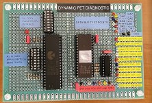
>>> Check the simple things first, oddly the jumpers on the two jumper blocks are incorrect for a 32k PET. On the 6 way block jumper D should be closed and on the 10 way block jumper k should be closed. You can solder those cut jumpers back together, the rest look correct.
@Hugo Holden
It is my assertion that links 'D' and 'K' are not actually used. Or (at least) I don't see them described on the schematics...
Dave
@Hugo Holden
It is my assertion that links 'D' and 'K' are not actually used. Or (at least) I don't see them described on the schematics...
Dave
")