| VCF West | Aug 01 - 02 2025, | CHM, Mountain View, CA |
| VCF Midwest | Sep 13 - 14 2025, | Schaumburg, IL |
| VCF Montreal | Jan 24 - 25, 2026, | RMC Saint Jean, Montreal, Canada |
| VCF SoCal | Feb 14 - 15, 2026, | Hotel Fera, Orange CA |
| VCF Southwest | May 29 - 31, 2026, | Westin Dallas Fort Worth Airport |
| VCF Southeast | June, 2026 | Atlanta, GA |
-
Please review our updated Terms and Rules here
You are using an out of date browser. It may not display this or other websites correctly.
You should upgrade or use an alternative browser.
You should upgrade or use an alternative browser.
Commodore 3016 scrambled screen
- Thread starter TheMatrix
- Start date
Hugo Holden
Veteran Member
Can you take a photograph to see which pcb variant you are dealing with ?
TheMatrix
Experienced Member
Can you take a photograph to see which pcb variant you are dealing with ?

Hugo Holden
Veteran Member
The picture, as usual, tells a 1000 words.
You have a Dynanic PET board with 32k of 4116 DRAM. Of which the upper 16k are in sockets. And your 2114 video RAMs not in sockets.
The glaringly obvious thing is that the CPU is in the wrong socket (assuming the IC without a label on it is a 6502 CPU at all), it should be in socket UC4 and the Rockwell 6522 should be in socket UC5. That should be remedied immediately.
A mistake like that suggests somebody has been pulling out IC's and just putting them back into sockets without thinking. Your ROM's could be mixed up too, so check carefully. It pays to check that you have the correct ROMs in the correct places by checking on Zimmers.
If still not working after that:
Check the simple things first, oddly the jumpers on the two jumper blocks are incorrect for a 32k PET. On the 6 way block jumper D should be closed and on the 10 way block jumper k should be closed. You can solder those cut jumpers back together, the rest look correct.
There are a few sources of unreliability on these boards which may or may not be affecting your board.
One is the white single wipe IC sockets. The are usually ok though if the IC's are re-seated so do that initially.
Most PETs repaired on the forum have had at least one faulty 2114 video RAM IC.
Often the ROM's are defective too. You can check these against the Zimmer's files. You need to be able to read the ROMs, a GQ-4x programmer can do it and can create new ROM's using the 2532JL and the 2716 UV Eproms.
The blue Tant capacitors are notorious for shorting out. And occasionally the VIA & PIA IC's are defective.
The best thing initially, is to run the board with the upper 16 k DRAM removed from the sockets, this removes some variables. Check the power supply voltages on the pcb from the 4 voltage regulators. Check that the 555 timer is producing a 1 second reset pulse at turn on and that there is activity on the CPU's sync pin 7.
After the basic checks are done, most people approach the repair by removing the VIA and PIA IC's to rule out more initial variables and running a NOP generator and PETTESTER system. Other fault finding methods can work depending on how familiar you are with digital logic and how handy you are with a scope.
Last edited:
TheMatrix
Experienced Member
TheMatrix
Experienced Member
Also checked the roms. They seems ok. i have read them with eprom programmer and compared it against the bin files on zimmers
Hugo Holden
Veteran Member
What happened with the screen image when the CPU was put in the correct socket?
Are the power rails checked yet ?
It is good there is activity on the sync pin, but one concern is that the CPU might be damaged by having been in the wrong socket. The CPU power pin is pin 8, but its pin 20 on the 6522 VIA, which could also be damaged as a result of the switch.
To be sure initially, it would pay to remove the VIA and the two PIA's and try another 6502 CPU, before moving on with the repair.
Each time a change is made you need to document the changes if any in the display. Once the faults are fixed these original parts can be plugged in later for testing.
I'm sure members Daver2 and Nivag can help you with their PETTESTERS & Romulators & NOP generator help. The fact that you had a screen display indicates that most of the circuitry in the master clock circuitry and logic that generates the H.drive and V.drive for the VDU is working which is a good start.
You should buy some 2114 Ram IC's now and a few spare 4116's, because you may end up needing them and these days things can take a while to arrive in the post. Most of the logic IC's on this board if they require replacing are easy to get on ebay, except for the MC3446 for the IEEE interface, but I know where some are if you get stuck later.
Last edited:
TheMatrix
Experienced Member
Hugo Holden
Veteran Member
I already tested with other CPU and 6522. Both of 2114 are defect. Tested with the RetroChipTester. Replaced now by other ones.
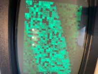
Now my screen is different.
Not surprising, most PET repairs seem to involve at least 1 defective 2114. Yet, it is interesting that most vintage 2114 SRAM IC's I have bought as spare parts and for other projects have been ok. I'm not sure why they appear to have a very high mortality rate in the PET.
Have you checked for a normal reset pulse out of the 555 yet ?
I think you did test the reset circuit, but also worth checking the gate on the output of the 555 too.
It may be time to make a NOP generator and Daver2's PETTEST ROM initially at least. This is the sort of screen that appears normally at boot up, for a second while the 555 is doing the reset, but I could be wrong and it could be some other screen variant.
Last edited:
daver2
10k Member
I agree, this now looks like the 'correct' random screen as opposed to the previous 'non random, random' screen (if you get my drift).
As Hugo has already stated, check the /RESET pulse at the CPU. I would also check the clock pins on the CPU.
After that, NOP generator (to test the address buffers and address decoder).
The we can move on to my PETTESTER. This will help us checkout the CPU to VIDEO interface. Then the RAM and ROM.
Dave
TheMatrix
Experienced Member
I have reset puls on 555 and CPU.
Clock is also present. Can i also first use the PETTESTER? i have download the bin and burned it on a 2716.
Is that correct?
Clock is also present. Can i also first use the PETTESTER? i have download the bin and burned it on a 2716.
Is that correct?
Last edited:
TheMatrix
Experienced Member
I also build the NOP generator from this page http://6502.org/mini-projects/nop-gen/nop-gen.htm
What's now the best way to use it?
What's now the best way to use it?
daver2
10k Member
Let's go for my PETTESTER code first since you have already burnt an EPROM.
A 2716 should be OK. Remove the existing EDIT ROM (from socket UD8) and install the PETTESTER ROM in it's place.
Did you download the PETTESTER documentation as well?!
Dave
A 2716 should be OK. Remove the existing EDIT ROM (from socket UD8) and install the PETTESTER ROM in it's place.
Did you download the PETTESTER documentation as well?!
Dave
TheMatrix
Experienced Member
I have placed the PETTESTER ROM in UD8
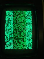
When i turn it on, i see same image as my last posted picture.
I have also the documentation
When i turn it on, i see same image as my last posted picture.
I have also the documentation
daver2
10k Member
Ok. Worth a go... Didn't pay off though...
Remove the CPU, install your NOP generator into the CPU socket (being careful not to damage the IC socket) and reinstall the CPU into the NOP generator.
Power up.
You should observe the address bus (on the CPU) with the oscilloscope as follows:
AB0 (pin 9) should be 250 kHz.
AB1 (pin 10) should be 125 kHz.
Every higher address pin should be half the frequency of the previous address pin.
If the CPU address bus looks OK, then check the outputs of C3 and B3 (buffered address signals BAn). These should all have the same frequency as the CPU address lines.
I would also check BPhi2 at the same time (1 MHz signal).
If all looks good - we can then test D2.
Dave
TheMatrix
Experienced Member
I think i need to build a other NOP Generator. I have build the one from http://6502.org/mini-projects/nop-gen/nop-gen.htm
There was no indication that i needed to have a socket on the NOP generator.
There was no indication that i needed to have a socket on the NOP generator.
daver2
10k Member
Ah, that is a NOP generator that plugs into an EPROM/ROM socket.
That will not work on a Commodore PET I am afraid...
The ROM sockets 'assume' that the buffered address lines work.
This adapter 'jams' the data bus with a NOP instruction $EA. Unfortunately, as the CPU accesses other parts of the PET (e.g. RAM, video RAM and the I/O space) they also write data onto the data bus to the CPU (because they are being accessed). This will result in bus contention, the CPU not necessarily reading a NOP instruction, and disappearing into the weeds...
Dave
TheMatrix
Experienced Member
Do you know where to find information on NOP Generator for 6502 socket?
daver2
10k Member
6502 NOP Generator - Platform for creating and sharing projects - OSHWLab
Whether you are sharing innovative hardware designs or finding design inspiration, this is the best place for you. From beginner to specialist, we can all communicate and learn together. We invite you to design and share with us.
If you have a spare 6502 CPU there is always this:

A NOP generator can be made from a 'socket sandwich'. All the pins from the top socket (where the CPU plugs in) are connected to the lower socket (that plugs into the CPU socket on the logic board) - with the exception of the eight (8) 6502 data bus pins (26 through 33 inclusive). These do NOT connect through from the top to bottom socket. The bottom socket does not have these pins connected at all. The top socket has the CPU data bus pins wired to form a NOP instruction = $EA = 1110 1010. A logic '0' being connected to 0V/GND and a logic '1' being connected to +5V/VCC.
D7 (pin 26) being a logic '1'.
D6 (pin 27) being a logic '1'.
D5 (pin 28) being a logic '1'.
D4 (pin 29) being a logic '0'.
D3 (pin 30) being a logic '1'.
D2 (pin 31) being a logic '0'.
D1 (pin 32) being a logic '1'.
D0 (pin 33) being a logic '0'.
You may require an intermediate IC socket to give you a 'gap' within which to perform the wiring.
I would also use a 1k pull-up resistor to +5V/VCC for the logic '1'.
Dave
I used two 'tulip' sockets, with pins soldered together, and made a NOP Generator that way. The 6502 clearly plugs into the top one and the bottom has those pin headers with the right pin-width to go into the socket on the board. Even then, I plugged another duel-leaf socket into the one soldered into the motherboard to protect it.
The end result is this "Tower of Power"")


The end result is this "Tower of Power"
Last edited: