• Please review our updated Terms and Rules here

Commodore 3016 scrambled screen

Here we go...

CPU pin 34 (R/W) should be HIGH. Only ever READ with the NOP generator.

Follow this signal through the logic gates:

A10/4 HIGH.
A3/12 LOW.
A3/8 HIGH.

CPU pin 39 (Phi2) should be a 1 MHz clock.

Follow this signal through the logic gates:

A10/8 1 MHz.
A10/2 1 MHz.

E9 and E10 pins 1 and 19 should both be pulsing.

Check pin 20 of all of the ROMs. They should be pulsing.

Check that I10 and I11 pin 1 are pulsing.

Check that I10 and I11 pin 19 are HIGH.

Check that I2 pin 3 is HIGH.

I2/4 is pulsing.

I2/15 is pulsing.

J2/15 is pulsing.

I2 pins 5, 7, 6, 12, 11, 10 and 13 are pulsing.

E7 and E8 pin 1 are pulsing.

E7 and E8 pin 19 are HIGH.

Check all of the signals identified as RDn and BDn on I10 and I11.

Check all of the signals identified as SDn and BDn on E7 and E8.

Check all of the signals identified as BDn and Dn on E9 and E10.

All signals should be either TTL high, TTL low or pulsing between TTL high and TTL low.

We are looking for nice (ish) signals. Unfortunately, vintage computers tend to have some horrid-looking signals at times, but they should definitely avoid the 1.0 to 2.5 Volt area. This would potentially indicate bus contention.

I am sure I have made the odd typo. above...

Dave
Checked most things. looks ok.
Now last part. But what dou you mean by this?:

Check all of the signals identified as RDn and BDn on I10 and I11.

Check all of the signals identified as
SDn and BDn on E7 and E8.

Check all of the signals identified as BDn and Dn on E9 and E10.


And typo here?

A10/4 HIGH.
A3/12 LOW.
A3/8 HIGH.


CPU pin 39 (Phi2) should be a 1 MHz clock.

Follow this signal through the logic gates:

A10/8 1 MHz.
A10/2 1 MHz.
 
Typo means that I have probably made a typographical error somewhere in the text of my post...

A3/12 LOW (etc.) means check IC A3 pin 12 for being a logic LOW.

RDn on I10 and I11 means that these are busses consisting of a bunch of signals (in this case RD0, RD1, RD2, ... RD7) going to ICs I10 and I11. If you look on the schematics - and find ICs I10 and I11 - you should observe the named bus signals, and which pins of I10 or I11 they connect to, so you can proble them individually.

Is my shorthand reasonably clear for some more probing?

I am on my phone at the moment, and I hate this virtual keyboard with a vengeance! Hence the reason I try to abbreviate the text a bit. Sorry for any confusion.

Dave
 
It’s clear now 😁. I thought I meant by A10 the port on the cpu. But you meant IC A10 😬. I will check everything again then.
And i also hate typing with phone🙃. Sometime it changes into text that make no sense
 
>>> It’s clear now.

Excellent. Sorry for any confusion.

>>> Sometime it changes into text that make no sense.

Tell me about it! I switched off predictive text, only then to get complete rubbish as the touchscreen is not very accurate! At least predictive text fixed the obvious rubbish - but then still leaves me with stuff that makes no sense, even though the words themselves are English!

Dave
 
Can you put the 2K PETTESTER EPROM you burnt into UD8.

Is it also possible to either burn a 2532 EPROM with the correct image for the KERNEL ROM (UD9). Either that, or verify the contents with the available image from the Zimmers website.

We need to see if we can get my PETTESTER running...

Dave
I have already checked the roms with the bin files on zimmers page.

The pettester is on a 2716 eprom. is that ok?
 
Ok, so the CPU is still executing instructions.

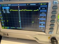
Can you can now check the OUTPUT pins of UD2 to see which pins are pulsing LOW. This will tell us what is being selected (ROMs, RAMs, screen etc).

Dave
 
I can't really tell much from that video I am afraid.

I suspect your timebase may be too fast also.

Dave
 
If PETTESTER is running I am expecting to see lots of activity on /SELE and /SEL8 (UD2 pins 16 and 9 respectively).

Alternatively, check pin 20 of the ROM sockets to at least see which ROM(s) are being accessed (if any).

>>> I think i first will check everthing again. To see that is not missed something.

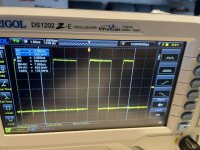
No problem. Just remember to adjust your oscilloscope timebase as required - because the activity may be quicker (or slower) than the timebase.

Dave
 
But nothing on pin 20 of UD8?

Permanent activity on UD8 pin 20 implies the code is 'stuck' within the Kernal ROM and is not doing what it is supposed to.

Corrupt Kernal ROM I am thinking?

Dave
 
Back
Top