daver2
10k Member
Why?
Dave
Dave
| VCF West | Aug 01 - 02 2025, | CHM, Mountain View, CA |
| VCF Midwest | Sep 13 - 14 2025, | Schaumburg, IL |
| VCF Montreal | Jan 24 - 25, 2026, | RMC Saint Jean, Montreal, Canada |
| VCF SoCal | Feb 14 - 15, 2026, | Hotel Fera, Orange CA |
| VCF Southwest | June, 2025 | University of Texas at Dallas |
| VCF Southeast | June, 2025 | Atlanta, GA |
I see strange signals and I can't understand where the fault could be..Why?
Dave

I will never be able to reach your level of expertise unfortunately, you could fix any computer!You missed I4 from the set of readings.
However, the results are consistent, but not correct.
I think I know what is going on, but I could do with some single channel oscilloscope traces of a number of pins to potentially rule out other causes.
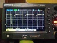
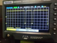
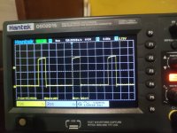
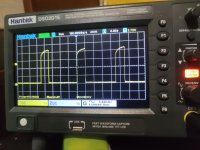
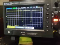
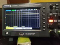
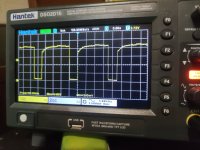
G7 pins 8, 9, 10 and 11.
B2 pins 9, 10, 11, 12 and 13.
A5 pin 3, 4, 5 and 6.
If these pins are correct I would suggest replacing I10 and I11. My thoughts are that some of the I10 and I11 buffers are writing to the DRAM when they should be reading. They may be reading as well of course, but (in this case) they will be reading what the write buffer is writing!
When you have replaced I10 and I11, do NOT install the DRAMs - but leave our resistors in place.
I will be very annoyed if replacing I10 and I11 does not fix the problem...
But PLEASE wait until after you have taken the measurements I have asked for and I have analysed your results.
Dave
I should look for connections with these pins, shouldn't I? But now I have to take care of some errands and I'll have to postpone the rest of the work until tomorrow..ok?Ignore it then - but you do know how to deal with this scenario - don't you? We came across this in a previous repair, so I shouldn't have to tell you a second time...
Dave
Ok thanks so much, tomorrow i ll remove these ics and i'll install two new sockets. Good night!Those signals look OK.
So I would now replace I10 and I11 tomorrow.
Dave