• Please review our updated Terms and Rules here

Commodore pet 2001-8 no video from logic board

When de-soldering be careful to not overheat the board at >350C the board might want to bubble and delaminate which would ruin your day. The safest approach is probably to cut the legs and do one pin at a time. Depending on your skill level it might be fun to try and get the device out to test it standalone but it might not be worth it!

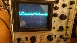
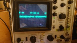
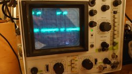
As I alluded to, my approach is to only remove the soldered in IC, when the detailed scope recordings of it in circuit, conclusively prove it is defective, beyond any doubt.

Then in this case, because nothing is lost, it is far better to cut the IC pins with very sharp needle nose cutters, close to the IC body and remove the pins, one by one from the pcb.

Then, after that is done add fresh solder to the pcb and then use the solder sucker to clear the holes and solder wick to remove lumpy solder from the pads and then clean up with IPA or better CRC's CO contact cleaner..

This way, the most valuable part you are working with ( which is the pcb not the IC's) is not damaged.

And if you have been diligent, you will not have unnecessarily sacrificed a good vintage IC, in the mistaken belief that it was defective.

If you get it wrong and you are back to square 1 and conclude that the original lovely vintage date code IC that you have just removed and cut the legs off, was in fact ok, then you only have yourself to blame by not being thorough enough with your oscilloscope tests and jumping to conclusions that it was defective.

Of course, to get it right "most of the time" it is a learning curve. It takes a long time to be close to 100% confident of your decisions in the area.

Therefore, if you foul it up and sacrifice a perfectly good IC, don't beat yourself up about it, but by the same token learn from it, don't make the same mistake next time.
 
I wouldn't disagree. Even if an output suggests a device may be defective then there is always the possibility something downstream is loading it incorrectly.

You should check voltages... Power and ground at the suspect device and, as suggested earlier, check on both DC and AC to get an idea about ripple.

My money is still on C9 though
 
Thanks for all the advice. You have all been a great help to me and I have enjoyed using the logic probe and recording my findings.
I would like to try the oscilascope next for some more tests before replacing 74LS93 at c9. I have ordered a couple of these just in case i need to change it.
The thought of removing a potentially working ic from 1977 does feel wrong.
If anyone has the patience to talk me through using the oscilascope sometime that would be great.
I will add a pic of my scope and model number tomorrow.

Frank.
 
If you look at the schematic for a while you will notice that although it is drawn in a confusing (IMHO) way what is happening is a 8MHz pixel clock is being successively divided down to the H sync clock, so by measuring the frequencies (you should get nice square waves on your scope) you can prove this is working (or not).

I don't think I am a 'collector' because I have no qualms with replacing components. In particular flip-flops and counters are common failures along with 6550s, 6540s, 6521s and sometimes even simpler gates.

@RGM if you are concerned with making hardware changes then I know someone who would do it for you for a small fee... ;)
 
Thanks for all the advice. You have all been a great help to me and I have enjoyed using the logic probe and recording my findings.
I would like to try the oscilascope next for some more tests before replacing 74LS93 at c9. I have ordered a couple of these just in case i need to change it.
The thought of removing a potentially working ic from 1977 does feel wrong.
If anyone has the patience to talk me through using the oscilascope sometime that would be great.
I will add a pic of my scope and model number tomorrow.

Frank.
You should be able to measure whether C9 is defective, or not with your oscilloscope. For any digital IC you are testing, it pays to look up its data sheet and logic diagrams.

The oscilloscope is the "window" that lets you see into the workings of both analog and digital circuits. Signals, be they rectangular waves in digital systems, or sinusoidal like or other waves in analog systems are often changing, repetitively over time.

The scope lets you see these dynamic waves (voltages) graphically and will give you the insight you need for fault finding complex analog or digital circuits.
 
Whilst you wait for the replacement device...

I made some traces for you..

C9 pin 1.... this is the 8MHz system (and pixel) clock.

C9p1.png

Note that this appears on my scope as something that doesn't look like a perfect square wave... factors like capacitance and drive in the circuit, scope bandwidth, probe compensation, shielding etc. all make this a bit less square than theoretical. But essentially we see 8MHz as expected.

C9 in 11...


C9p11.png

pin 11 shows the output of the divide by 8 part (Q1, Q2, Q3 clocked by nCP1)

8MHz divided by 8 = 1MHz which is what we see.

C9 pin 12

C9p12.png

The signal then feeds into Q0 clocked by nCP0 to give another divide by 2.

We see 500kHz on pin 12. This is the signal you have missing with your logic probe.

Continuing on....

B5 pin 12

B5p12.png

Again Q0 and nCP0 used to create a divide by 2... we are now down to 250kHz... then this is fed into the other part of the counter...

B5 pin 9

B5p9.png

Another divide by 2 to 125kHz

That's enough for now... you need to fix the 74LS93 at C9 :)
 
DSC_0525.JPGGot my ancient scope setup and it has been very helpful seeing the activity in some of the logic. Pictured is the readout from C9 pin 1.
I will report more of my findings once I have more time over the weekend.
I have a query about the circuit diagram.
I have just been tracing vertical pin 3 from j7 and it takes me to pin 11 of D7 and not D8 which the circuit diagram illustrates.
I guess this a location mistake in the diagram of the board.
 
Last edited:
Whilst you wait for the replacement device...

I made some traces for you..

C9 pin 1.... this is the 8MHz system (and pixel) clock.

View attachment 1247837

Note that this appears on my scope as something that doesn't look like a perfect square wave... factors like capacitance and drive in the circuit, scope bandwidth, probe compensation, shielding etc. all make this a bit less square than theoretical. But essentially we see 8MHz as expected.

C9 in 11...


View attachment 1247838

pin 11 shows the output of the divide by 8 part (Q1, Q2, Q3 clocked by nCP1)

8MHz divided by 8 = 1MHz which is what we see.

C9 pin 12

View attachment 1247839

The signal then feeds into Q0 clocked by nCP0 to give another divide by 2.

We see 500kHz on pin 12. This is the signal you have missing with your logic probe.

Continuing on....

B5 pin 12

View attachment 1247840

Again Q0 and nCP0 used to create a divide by 2... we are now down to 250kHz... then this is fed into the other part of the counter...

B5 pin 9

View attachment 1247841

Another divide by 2 to 125kHz

That's enough for now... you need to fix the 74LS93 at C9 :)
Very helpful thanks.
 
I have just been tracing vertical pin 3 from j7 and it takes me to pin 11 of D7 and not D8 which the circuit diagram illustrates.
I guess this a location mistake in the diagram of the board.
Not sure.
The vertical drive is driven from C9 pin 8... it would be interesting if you find life.
 
I do get readings on the scope from J7 pin 1 pin 3 pin 5 but not at the suggested settings in the schematics display circuit.
Here is what I get with the settings I used in order from left to right. Left pic being pin 1 on J7. As you can see no square waves at all.DSC_0529.JPG
 

Attachments

  • DSC_0531.JPG
    DSC_0531.JPG
    3.3 MB · Views: 4
  • DSC_0530.JPG
    DSC_0530.JPG
    3.3 MB · Views: 5
Is your probe on x1 ? You also need to have 1V/div or similar as you did in your first picture. The other signals look like mV?
 
Is your probe on x1 ? You also need to have 1V/div or similar as you did in your first picture. The other signals look like mV?
Ok so in this pic connected to pin 1 of C9 using left ch probe x1 v/div 1, time/div .5us which I assume is nanoseconds.
All previous pics where obtained with the previous settings other wise I just got flatlined.
 

Attachments

  • DSC_0533.JPG
    DSC_0533.JPG
    3.1 MB · Views: 3
ll previous pics where obtained with the previous settings other wise I just got flatlined.
Exactly. If you have time on your hands... You can look at the processor.... Check Reset and see what happens on power up.

If C9 is dead as suspected you would not see a phi2 so the processor will not be running.
 
Exactly. If you have time on your hands... You can look at the processor.... Check Reset and see what happens on power up.

If C9 is dead as suspected you would not see a phi2 so the processor will not be running.
Ok so I should leave scope at these new settings going forward? My probe does not have X1 or x10 only an adjustment screw. The scope has X1 or X5
 
Ok so I have replaced C9 sn74ls93n and I am now seeing a horizontal line on the screen. Yay!
I have taken some readings from J7 with the scope.
Pic 1 video pic 2 vertical pic 3 horizontal.
Getting square waves now but vid signal looks small compared to the image in the schematic?
 

Attachments

  • DSC_0577.JPG
    DSC_0577.JPG
    2.9 MB · Views: 6
  • DSC_0578.JPG
    DSC_0578.JPG
    2.7 MB · Views: 7
  • DSC_0579.JPG
    DSC_0579.JPG
    2.9 MB · Views: 8
  • DSC_0570.JPG
    DSC_0570.JPG
    2.4 MB · Views: 8
Ok so I have replaced C9 sn74ls93n and I am now seeing a horizontal line on the screen. Yay!
I have taken some readings from J7 with the scope.
Pic 1 video pic 2 vertical pic 3 horizontal.
Getting square waves now but vid signal looks small compared to the image in the schematic?
You are not making a recording of the vertical drive signal (if it is there ) yet, because in the three photos the scope timebase looks like its set on 20 uS/division.

To see the vertical pulses the timebase needs to be slowed right down because the spacing between the pulses is about 16.67 mS, so set the timebase for 5mS/division (or similar) when checking for the vertical pulses.

Make sure to have the scope's probe input on DC coupling (looks like it is), and set say for 2V/large division on the attenuator with a x1 probe, or if its a x10 probe set it for 0.2v/large division, which gives 2V/ large division with the x10 probe (a large division is usually a centimeter on the screen of most scopes). To be sure you have got that right, connect the probe onto the 5V supply and the trace should jump up by 2.5 large divisions = 5V.
 
Back
Top