• Please review our updated Terms and Rules here

KIM-1 repair

This is always an issue. The fact that you have replaced the CPU, indicates that you or someone before you has desoldered the original CPU.
The boards these were made from were really cheap. Before doing anything else, run through with an ohm meter for each pin, top and bottom. I'm an experienced person with a soldering iron. I had to repair one trace on my board so expect to check them all.
Are any of the other chips on sockets? The same thing. They need to be checked. To my knowledge, no KIM-1 ever had sockets from the factory.
If that is all ok, we need to go to a meter or a scope.
Check that things that Dave has listed.
The board has a mixture of TTL and MOS inputs. An open TTL input is a soft pull up of about 2.5 to 3 volts on a meter.
Since I assume the CPU is socketed, lets start by pulling it. The first test only needs the processor running, a working address buss, data bus and no extra things like interrupts going in.
I assume you have a schematic to look at ( http://www.zimmers.net/anonftp/pub/cbm/schematics/kim-1/kim.gif works well enough.
The debug board must be the boot code. This means the jumper need to make the KIM-1 work without the debug board, needs to be disconnected.
That is, no jumper tie on pin K. That is replaced with the switch labeled DB.
With the CPU removed check the pin on the address decoder, U4, inputs, 12, 13, 14, 15. They should all be "1". I will call any thing of 2or more volts a "1".
Now do the same for U4's outputs, pins 1 to 7 are "1". Pin 9 should change with the DB switch on the debug board. When "1" the debug board take over the
source of the boot code.
After things have been powered with the CPU removed for a while, do a temperature check of all the parts, nothing should be particularly hot.
Once past that, we can look at other things. As I recall, the Debug board doesn't need much other than a working address bus and data bus to do the first test.
Also, note that the switches on the debug board are not in a friendly order. Don't use the switches position numbers, note the schematic.
 
Just returned from the bar... you tell me if it's a good idea to work on this right now :)

U1-U3 are socketed, nothing looks like it has ever been worked on

I would check U1 (CPU) pins 2, 4, 6 and 40 for being HIGH.
SYNC is pulsing, 2, 4, 6 and 40 are HIGH

With the CPU removed check the pin on the address decoder, U4, inputs, 12, 13, 14, 15. They should all be "1". I will call any thing of 2or more volts a "1".
Now do the same for U4's outputs, pins 1 to 7 are "1". Pin 9 should change with the DB switch on the debug board. When "1" the debug board take over the
source of the boot code.
With the CPU removed, I assume you mean U4 on the KIM-1 and not the debug board
12 goes from low to high depending on DB switch of the board
13, 14, 15 are at 1V, they don't change state at all
Pin 9 behaves as pin 12, changing state depending on whether DB is 1 or no
Pin 2 and 3 are low, rest (1, 4-7 are HIGH)

Do I have a faulty U4 / 74LS145N?

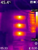
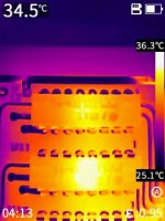
Attached a picture of some ICs.. nothing gets hotter than 50 °C, one of the RAM chips is cold, interestingly.

WIll be gone for the weekend, but looking forward to continuing Sunday evening


THanks for your help!
 

Attachments

  • IRI_20240705_053352.jpg
    IRI_20240705_053352.jpg
    252.5 KB · Views: 7
The K1 is not used on the KIM-1. It only goes to the edge connector for expansion. The 74145, pin 2, has a open collectors so that pin is undriven and should also be low, with no pullup.
Pin 1 is K0. It has a pullup and drives directly to the pin 13's of the RAMs. The fact that one RAM looks dead is a good indicator that it might be pulling the K0 line down.
I'd recommend pulling that RAM and see if it will run the first diag test again.
I don't think U4 is bad, at least it doesn't look to be the root cause. It responds correctly to the DB switch.
The first test doesn't need anything other than CPU and clocks to run. Since U2 and U3 are socketed, they can be pulled, while running the first test.
Make sure to note where pin 1 is, they are not logically placed.
Dwight
 
Once you get it working, note that most of the test are quite small in code space. The EROM on the diagnostic board has 5 completely unused 1K blocks that can be used.
Even the test 1K blocks have a lot of unused space. With the DB switch off, it will boot to the monitor and you can then run your favorite program in one of the empty EROM spaces.
The astroids program that I have in the one bank is just Butterworth's program, relocated to run in the EPROM space.
Dwight
 
I've pulled the U7 RAM, U2 and U3.
It's trying to do something, but still not getting there.

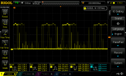
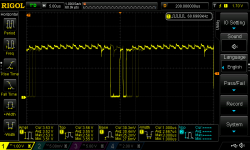
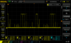
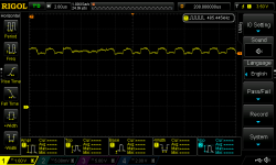
I attached some scope pictures. Maybe you can make some sense of it.
Nothing looks suspicious on the thermal camera. U4 13, 14, 15 are still at about 1V with the CPU removed.
Regarding pin 13 on the RAMs, they're all low except U5 and U7 (now empty), with the CPU removed
 

Attachments

  • A4.png
    A4.png
    42.2 KB · Views: 2
  • D.png
    D.png
    49.7 KB · Views: 2
  • D0.png
    D0.png
    44.1 KB · Views: 2
  • D7.png
    D7.png
    45.8 KB · Views: 2
  • U4-15.png
    U4-15.png
    39.1 KB · Views: 2
The processor looks to be trying to run. I'm assuming picture U4 is with the processor in place. There is not a lot of information with each picture, about the conditions.
Please do a little better. What are the total conditions for each picture. In your text you state the CPU is removed? is that true?
Back to U4. If pin 13 is still not above 2.5V , With the CPU removed, there is likely still something pulling it down.
U4 pin 1 has a pullup resistor R35 of 560 ohms.
The possible problems are:
U4 pin 1
U16 pin 1
U5-U12 pin 13
With the CPU removed, pin 13 of the RAMs should be Hi while pin 12 of U4 is high.
I assume U7 was the one RAM that was cold. So with that removed, it is not the ONLY problem. It was clearly not acting right, compared to the other RAMs. Don't expect much from it.
Don't expect anything predictable to be happening of the processor to boot with one or more of the RAM pulled or bad, using the CPU and code in U2.
The RAMs each do only one bit of the data bus and like I said,
the processor is basically brain dead with out page 0 and page 1 RAM, completely working.
Don't bother trying to get something useful happening without RAM, other than the first test.
My first diagnostic program does not use any RAM so it is the only step in the diagnostic that.
Not seeing pin13 of the RAMs, not a solid logical 1 is bad. Something is pulling the line down. It could be any of the other RAMs that you haven't removed or U4, or U16.
The above list are the only things connected to the K0 line. Before pulling every RAM, you might try using a ~500 ohm resistor to pull up and down on each DO ( data out ) pin 12
of each RAM. Conditions being power up with the U1, U2 and U3 all removed. Just get a list of voltages those RAMs that are still on the board, connecting the resistor free end to ground and then to 5v, board powered on. I don't expect this to show much but it is worth a try before pulling other parts of the board.
Do look at R35 and make sure it isn't physically broken, first.
Finding the culprit with out special current sensing devices is not going to be easy, other than pulling one part at a time. HP made just such a probe. I played with it a little but the probe was several thousand dollars and not in our departments budget.
Pulling U7 was the most likely. Of course, all the other RAMs could be bad and U7 was the only good one. At this point were are looking for a needle in a hay stack.
Dwight
 
I have faced the problem before where it could be one of a number of RAMs defective, and they are soldered in. How to find them, when as Dwight puts it the processor is brain dead without page 0 ?

The trick I used was to dynamically disable the page 0 ram, with an address decoder, but a little more maybe the lower 1k and at the same time that was electrically disabled, gate in a known good SRAM. I am not sure how this could be done on a KIM-1 as I have not investigated it for this computer, but the idea worked very well for a PET to find and isolate the defective 4116 Drams. Once the computer boots with substitute SRAM, small programs can be run to interrogate the the existing faulty RAM IC array and figure out which ones are the duds.
 
The processor looks to be trying to run. I'm assuming picture U4 is with the processor in place. There is not a lot of information with each picture, about the conditions.
Please do a little better. What are the total conditions for each picture. In your text you state the CPU is removed? is that true?
Sorry about that, the pictures are with the CPU in, the measurements where it says it was removed where without, otherwise with it running
Back to U4. If pin 13 is still not above 2.5V , With the CPU removed, there is likely still something pulling it down.
U4 pin 1 has a pullup resistor R35 of 560 ohms.
The possible problems are:
U4 pin 1
U16 pin 1
U5-U12 pin 13
With the CPU removed, pin 13 of the RAMs should be Hi while pin 12 of U4 is high.
I assume U7 was the one RAM that was cold. So with that removed, it is not the ONLY problem. It was clearly not acting right, compared to the other RAMs. Don't expect much from it.
I'll check that tomorrow
Don't expect anything predictable to be happening of the processor to boot with one or more of the RAM pulled or bad, using the CPU and code in U2.
The RAMs each do only one bit of the data bus and like I said,
the processor is basically brain dead with out page 0 and page 1 RAM, completely working.
Don't bother trying to get something useful happening without RAM, other than the first test.
My first diagnostic program does not use any RAM so it is the only step in the diagnostic that.
Yup, understood that... I'm trying to make the LED blink before I look at fixing RAM issues
Not seeing pin13 of the RAMs, not a solid logical 1 is bad. Something is pulling the line down. It could be any of the other RAMs that you haven't removed or U4, or U16.
The above list are the only things connected to the K0 line. Before pulling every RAM, you might try using a ~500 ohm resistor to pull up and down on each DO ( data out ) pin 12
of each RAM. Conditions being power up with the U1, U2 and U3 all removed. Just get a list of voltages those RAMs that are still on the board, connecting the resistor free end to ground and then to 5v, board powered on. I don't expect this to show much but it is worth a try before pulling other parts of the board.
Do look at R35 and make sure it isn't physically broken, first.
R35 is ok. I'll try to get some results with the resistor.
Finding the culprit with out special current sensing devices is not going to be easy, other than pulling one part at a time. HP made just such a probe. I played with it a little but the probe was several thousand dollars and not in our departments budget.
Pulling U7 was the most likely. Of course, all the other RAMs could be bad and U7 was the only good one. At this point were are looking for a needle in a hay stack.
Dwight
I've read about the probe, but good luck finding one... you've confirmed my suspicions, that it is finding a needle in a haystack but I'll try my best narrowing it down before starting to snip off legs.
I have faced the problem before where it could be one of a number of RAMs defective, and they are soldered in. How to find them, when as Dwight puts it the processor is brain dead without page 0 ?

The trick I used was to dynamically disable the page 0 ram, with an address decoder, but a little more maybe the lower 1k and at the same time that was electrically disabled, gate in a known good SRAM. I am not sure how this could be done on a KIM-1 as I have not investigated it for this computer, but the idea worked very well for a PET to find and isolate the defective 4116 Drams. Once the computer boots with substitute SRAM, small programs can be run to interrogate the the existing faulty RAM IC array and figure out which ones are the duds.
This is a cool idea... I don't know how common multiple faults are on KIM-1s.. mabye it is worth looking into?
 
This is a cool idea... I don't know how common multiple faults are on KIM-1s.. mabye it is worth looking into?

When I was pondering the problem I realized that to dynamically isolate the computer's RAM all that had to be done was to inhibit its Reads, It didn't matter about Writes. So it was a mater of just preventing the tristate buffer from putting the RAM data onto the Bus, over the specific address range. Turned out to be easy in the PET because there was a gate that was begging to be disabled, but it would have worked just as well by lifting the control line on the buffers. One way to do that sort of thing without any pcb or IC damage is to just solder-suck the /E pin and free the it in the hole and get it to disconnect and then you can solder a wire to the projecting pin to gain control over the buffer, later you can just re-solder the pin.

That same address decoder output inhibiting the reads was then used to switch SRAM onto the memory expansion connector.

In any case the method does work, it is explained in this article. The idea would need to be adapted to suit the KIM:

www.worldphaco.com/uploads/DRAM%20MEMORY%20TEST%20SYSTEM%20FOR%20THE%20DYNAMIC%20PET%20COMPUTER.pdf

One other reason to do it, in the PET's case, was that the computer once functioning allowed investigations of the DRAM support circuitry with the scope with the computer running on SRAM . For computers with SRAM only memory this wouldn't matter because there is none of the elaborate DRAM support circuitry present to investigate.

I found with this system also that when the RAM was normal, it outputs exactly agreed with the SRAM and they could actually run at the same time over the same address range without corrupting the computer's functions.
 
Alright, some progress I think?


IRI_20240711_041349.jpg

Pin 12 of U12 was stuck at 3 V and it was about 2 °C colder than the other chips.. not very scientific method but out it goes

It still doesn't execute code. U4 pins 12-15 are still at 1 V, even with the debug board out. With the CPU and the board in U4 12, 13 are low and 14, 15 look like the U5 15 picture in #25

If I understood the schematic correctly, there isn't much left on A10-A12 besides CPU itself

EDIT: K0 / pin 13 of the RAMs are at 5 V, I think on my previous measurements I got something wrong due to corrosion on the IC legs
 
Last edited:
Other things, did you check that you have clocks and the rest of things that Dave suggested.
I guess the next thing is to check that the RAMs are not blocking the bus. Although, a bus buffer could fail lets just check that the buffers are not being told to drive the bus.
Measure pin 6 of U15. It should be a logical 1.That doesn't mean there isn't a problem with a stuck output but we can look at that later.
W know from the thermal image that at least one RAM was bad.
One thing we haven't checked and that was that there was on error on the Debug board.
Remove U1, U2 and U3. Also remove the EPROM on the debug board.
Powered down.
We are going to check a bunch of KIM to debug board connections with an ohm meter.
Start with probes from the U1 to the EPROM socket of the debug board. Check all the data, D0 to D7, and address pins, A0 to A9.
When doing this, also make sure there is no adjacent pin shorts.
Now power up the KIMand debug board. ( parts in sockets yet )
With a scope probe look to see that there is a reset pulse at the 74LS74 pin 1.
Not sure if these two LED lighting will work. I think one of the data bits needs to be high or low to light the green LED. I need to get my boards and check these.
With a grounding wire, momentarily ground debug U2 pin 4. The red LED should light.
Do the momentarily ground U2 pin 1. The green LED should light. ( I forget the level of data bit of the bus try pulled up and pulled down )
The KIM reset switch should turn both out.
With the test pattern select switches in the first pattern check that EPROM pins 21, 23, 26 and 2 are 0 level.
If we get past that I'll have some more to check. It is going to be slow but "that is the way".
Dwight
 
Pin 6 of U15 is at logical 1, nothing is shorted on the EPROM socket and the select switches switch corectly at EPROM pins 21, 23, 26 and 2.
There is a reset pulse on 74LS74 pin 1

The LEDs don't light up when the 74LS02 Pin 1 or 4 are pulled up (they are already low). They light up on diode test so they're not faulty.

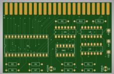
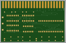
I am uncertain if I correctly assembled the debug board. The blog post http://retro.hansotten.nl/6502-sbc/kim-1-manuals-and-software/kim-1-diagnostic-board/ has two schematics. I looked at the first picture (http://retro.hansotten.nl/wp-content/uploads/2021/12/FAoPOmqXEAAOZxe-scaled.jpg) and assembled the board like that, but when scrolling down there is a second schematic (http://retro.hansotten.nl/wp-content/uploads/2024/01/KIM-1.debug_.pdf.01-scaled.jpg), which contains a U5?

The PCB I ordered has the EPROM marked U1, the 74LS02 as U2, 74LS04 as U3 and 74LS74 as U4 (at least that's how I put it together)

1720723864604.png 1720723889843.png

I'll try to find out if this matches the first schematic

EDIT: Yes the clock and other CPU related things appear to be fine
 
Last edited:
Pin 6 of U15 is at logical 1, nothing is shorted on the EPROM socket and the select switches switch corectly at EPROM pins 21, 23, 26 and 2.
There is a reset pulse on 74LS74 pin 1

The LEDs don't light up when the 74LS02 Pin 1 or 4 are pulled up (they are already low). They light up on diode test so they're not faulty.

I am uncertain if I correctly assembled the debug board. The blog post http://retro.hansotten.nl/6502-sbc/kim-1-manuals-and-software/kim-1-diagnostic-board/ has two schematics. I looked at the first picture (http://retro.hansotten.nl/wp-content/uploads/2021/12/FAoPOmqXEAAOZxe-scaled.jpg) and assembled the board like that, but when scrolling down there is a second schematic (http://retro.hansotten.nl/wp-content/uploads/2024/01/KIM-1.debug_.pdf.01-scaled.jpg), which contains a U5?

The PCB I ordered has the EPROM marked U1, the 74LS02 as U2, 74LS04 as U3 and 74LS74 as U4 (at least that's how I put it together)

View attachment 1282871 View attachment 1282872

I'll try to find out if this matches the first schematic

EDIT: Yes the clock and other CPU related things appear to be fine
I got my signals mixed up. I said I wasn't sure about the signals.
I was trying to get a clock pulse to the flipflop.
New instructions:
Nothing in the KIM sockets U1, U2 and U3. All connected and powered on.
Attach a ground connection pin 2 of the 7402. Now, momentarily pull pin 5 of the 7402 to ground.
That should light the Red LED.
With the ground still on pin 2, momentarily ground pin 3. The Green LED should light.
If not there is something wrong. All three schematics should work the same, at this point.
Of the lower ones, the left one should be the same as your board. The top one should be the same as well.
The only difference I see is the lower right one has a buffer to drive the LEDs instead of directly driving the LEDs from the flops.
Lets get past the LEDs first.
It might help to see a picture of your setup.
I'll try to check things in the morning, seeing that you are on the other side of the pond.
Dwight
 
Last edited:
You don't have to change your schedule for me... (today *I* have time in the morning)

Debugging the debug board: Pin 2 of 7402 is already at ground level.. grounding pin 3 makes pin 1 go high but otherwise not much is happening.

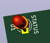
I toned out the LEDs found out that the round pads go to one end of R7 / R8, while the square ones go to the flip flop

I fell for it... I always assumed the square pad is the positive side but it looks like for LEDs it is not!

1720771007809.png

I swapped them around and with the CPU in, the LEDs are now lighting up (first test passes).

With some spare RAM (only 2 left in my stash unfortunately) I filled the gaps.. the RAM test fails at D2 (third blink).

Any tips how to find out which RAM could be faulty now?
 
The square pad in KiCad is the same end as the 'flat' on the LED which is the cathode = negative.

I try to make it very difficult for an assembler to get it wrong by ensuring that the silk screen mask correctly shows the outline of the LED itself - especially the flat.

Before assembling any PCB myself, I do a double-check to make sure I understand how every polarised component (LED, diode, transistor, tantalum bead capacitor etc.) is oriented. It is amazing how sometimes you have to do some 'reverse engineering' of the PCB tracks to work this out.

Dave
 
One thing about " cathodes and anodes", be it LED's, Vacuum tubes etc, a useful rule of thumb is "Positive emerges at the Cathode".

This was in line with what is known as "conventional current" which flows from positive to negative, but we all know the electrons themselves flow in reverse from negative to positive.

(However the idea of conventional current became entrenched in electrical engineering to the point that it became impossible to get rid of it, though oddly it was very useful explaining semiconductor behavior where 'holes" with a positive charge move in the opposite direction to electrons).

This takes into account devices being polarized by a power supply. So , for example, if you apply positive of a supply to the Anode of an LED (or the anode of any diode or vacuum tube) it will "appear" at the cathode and then to complete the circuit; the cathode connects to negative of the supply (of course by a resistor in series that limits the current).

The only time that rule appears to go counter intuitive is with zener diodes, that are wired in reverse to this rule, because they break down to a stable voltage drop, with reverse polarity applied.

As noted the flat on the plastic package of LED's is the LED's "cathode", equivalent to the black line marking on glass diodes or the silver line on diodes in epoxy packages.

Just to fool people the terminology of anode and cathode is a little different as applied to the source of power, such as a battery, because of the anions and cations at those terminals. The anode is the negative electrode were there is a surplus of electrons (the anode supplies electrons to the external circuit) and the cathode of the battery the positive terminal accepts electrons. Conventional current flows from the cathode of the battery to the anode, but the electrons flow from the anode to the cathode.

So lets say you have a battery and a resistor and an LED: You connect the "cathode" of the battery (+Ve) to the anode of the LED and then connect the anode of the battery (-Ve) to the cathode of the LED (and have a current limiting resistor in series with the hookup). It is these sorts of switch arounds with anode/cathode terminology that get very confusing for people hooking things up.
 
It sure confused me, but I now know I have to pay closer attention when I have to deal with anodes and kathodes...

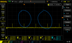
I had a look at D2 / U10, pins 11 of the RAM ICs.. they all trigger correctly with visible signals on the scope, except U10 where the signal is only a faint pulse (see circled in scope picture).

1720795660273.png

Is it another possible failed RAM or could it be something else? The signals on U13 don't look "wrong"...
 
It sure confused me, but I now know I have to pay closer attention when I have to deal with anodes and kathodes...

I had a look at D2 / U10, pins 11 of the RAM ICs.. they all trigger correctly with visible signals on the scope, except U10 where the signal is only a faint pulse (see circled in scope picture).

View attachment 1282926

Is it another possible failed RAM or could it be something else? The signals on U13 don't look "wrong"...
The signals there are not normal though it could be for more than one reason. They are sub-logic threshold level at less than one volt.

But they are narrow too and sometimes because of the sample rate settings narrow pulses can look lower in level than they are on the display, often when that happens though the amplitude of consecutive pulses appears to vary depending on where on the narrow pulse they get sampled, so that may not be a factor as they look uniform in level.
 
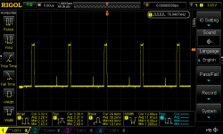
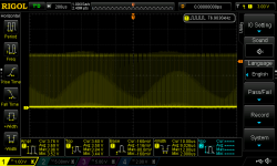
Could be that I'm measuring it wrong, but there are a lot of reflections or noise in the signal... I attached the ground to a leg of a capacitor nearby

Some signals look better than others, e.g. U12 pin 11. With slower timebase, there's some funny patterns

1720817454090.png 1720817503180.png

I'm waiting for additional opinions if U10 could be at fault or not. If it points towards this IC, I'll remove it and swap it with another one to see if the fault follows the IC
 
You don't have to change your schedule for me... (today *I* have time in the morning)

Debugging the debug board: Pin 2 of 7402 is already at ground level.. grounding pin 3 makes pin 1 go high but otherwise not much is happening.

I toned out the LEDs found out that the round pads go to one end of R7 / R8, while the square ones go to the flip flop

I fell for it... I always assumed the square pad is the positive side but it looks like for LEDs it is not!

View attachment 1282904

I swapped them around and with the CPU in, the LEDs are now lighting up (first test passes).

With some spare RAM (only 2 left in my stash unfortunately) I filled the gaps.. the RAM test fails at D2 (third blink).

Any tips how to find out which RAM could be faulty now?
Progress!
The schematic shows D2 as being U10. The test sequences across the RAMS. I don't recall which way it went across the board. Looking at my instructions I seemed to have left that part out of the instructions. I'm relatively sure I'd have started the read out scan at D0. I recall, which ever way it was made sense in the program. Going high to low might be easier to program.
The parts are tolerant to have a pin grounded. You should be able to see which end, it sequences from, by grounding the end output or the next to the end. The new fail should tell you which end things count from. The output pin is 12 on the RAMs. You might have to do one of the two end ones because of the patterns used and pattern that failed.
It does 2 passes if there isn't an error on the first pass it will go to the second. I don't recall which order it was but it was one pattern was one pattern was 55h and the other was AAh.
Not a really sophisticated test but you have to realize you can't test the RAM and use the RAM in a program. I used all the registers, including the stack pointer.
If the first pass fails, it doesn't go on to the second pattern. ( again, limited ability to do much more).
Although, it doesn't sound like this case, if it alternates pass, fail, pass, fail etc, it indicates the the bus driver is likely at fault. Again, think about the two patterns.
Anyway, grounding an output of known good RAM will tell you which way it scans across the board.
I'm not sure which RAMs you have. The original boards may have used 6102s but 2102 work fine. I think that was just a manufacture choice.
As for the board having a square pad for the LED, I don't think my original one had a square pad at either end. The flat on the LED went the to TTL output as it was to turn on with a pulldown.
Dwight
 
Back
Top