• Please review our updated Terms and Rules here

Memory problem with PET 2001

>>> I haven't had a chance to try any of the suggestions, but just wanted to resolve your confusion due to my less-than well-organized post above. The /CS trace above wasn't taken with the NOP generator in place, it was with the CPU set up regularly. I just included it as an example of what I was seeing on the kernal ROM when the board was trying to boot. No activity on the other ROMs.

That's OK - I just want to be clear in my mind under what conditions the various traces were taken under (as this matters in deciphering what we are seeing).

The NOP generator will demonstrate that the CPU/address buffers and chip select decoder is operational - as it doesn't involve the CPU executing instructions out of a ROM (we are forcing the data bus with a NOP = $EA).

My PETTESTER will demonstrate that the Kernal ROM and PETTESTER ROM will either work or not. If it doesn't work - the next question is what is the CPU actually executing (if anything)?! In this case have a look at the CPU SYNC pin (pin 7). If this pin is not pulsing high (it does this for every CPU instruction executed) the CPU isn't executing instructions at all (or was and stopped) indicating a problem with decoding $Fxxx and/or $Exxx. In this case we can monitor /SEL E and /SEL F - along with SYNC and /RESET (triggering on /RESET) to see what happens for the first few tens of instructions following a reset or power-up condition- and if it goes into the weeds or not.

If the CPU is still executing instructions - is it doing so within $Exxx (PETTESTER) or $Fxxx (Kernal ROM). The first is correct, the second not.

Executing the BASIC ROMS themselves just means that there are plenty of places for it to go into the long grass and die...

Dave
 
Ok, I made some actual positive progress today. I got an inexpensive logic analyzer and hooked it up to the Kernal ROM address lines. Output with NOP generator in place was as expected. Running the ROM code gave the following result after a reset:
View attachment 65735

Basically, it went to 0xFFFC and 0xFFFD, got the address 0xFFFF from there and then went off and died somewhere in the top of the Kernal ROM. I had previously verified my burned Kernal ROM against the file on my hard drive and even burned another. I went to check the file and it turns out that the whole last 2k of the file had been overwritten as 0xFF, and that was what was on the ROM. I had previously burned a good ROM that got zapped (put in the socket backwards) and I burned the replacement with the bad data. So a big issue solved. Here's the logic analyzer traces of the PETTESTER ROM actually getting selected after a reset.
View attachment 65736

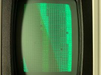
But I was still getting garbage on the screen. I started at the screen RAM address multiplexers and noticed that the BR/W signal was stuck (can't remember if low or high, but I think low.) So I traced that back all the way to the CPU and found that pin 34 was not making contact with the socket. I had replaced this socket with a new round pin one so I was surprised. I guess taking the CPU in and out, putting in the NOP generator, putting the ROM/RAM board in, etc., wore it out. I'll have to replace the socket, but for now I have adjusted the pin a little so it makes contact. Finally output from PETTESTER on the screen again. Not showing a working machine, but I'll take it for now.
IMG_7201-2.jpg

So I will now return to debugging the RAM, the original problem.

Thanks again for your help, suggestions and encouragement,
Greg


>>> I haven't had a chance to try any of the suggestions, but just wanted to resolve your confusion due to my less-than well-organized post above. The /CS trace above wasn't taken with the NOP generator in place, it was with the CPU set up regularly. I just included it as an example of what I was seeing on the kernal ROM when the board was trying to boot. No activity on the other ROMs.

That's OK - I just want to be clear in my mind under what conditions the various traces were taken under (as this matters in deciphering what we are seeing).

The NOP generator will demonstrate that the CPU/address buffers and chip select decoder is operational - as it doesn't involve the CPU executing instructions out of a ROM (we are forcing the data bus with a NOP = $EA).

My PETTESTER will demonstrate that the Kernal ROM and PETTESTER ROM will either work or not. If it doesn't work - the next question is what is the CPU actually executing (if anything)?! In this case have a look at the CPU SYNC pin (pin 7). If this pin is not pulsing high (it does this for every CPU instruction executed) the CPU isn't executing instructions at all (or was and stopped) indicating a problem with decoding $Fxxx and/or $Exxx. In this case we can monitor /SEL E and /SEL F - along with SYNC and /RESET (triggering on /RESET) to see what happens for the first few tens of instructions following a reset or power-up condition- and if it goes into the weeds or not.

If the CPU is still executing instructions - is it doing so within $Exxx (PETTESTER) or $Fxxx (Kernal ROM). The first is correct, the second not.

Executing the BASIC ROMS themselves just means that there are plenty of places for it to go into the long grass and die...

Dave
 
I changed the pullup resistor on /INIT from 1k to 75 ohms and that gets the voltage to about 4.75 V I think. Do you think this is ok? If I think about it more, I think I like the idea of wiring it directly to Vcc better. The resistor looks tidier, but maybe cutting the trace to pin 21 and running the bodge on the bottom of the board would be ok too. God knows it will have company from all of the corroded traces I had to fix.

Cheers,
Greg
 
Most things have a logical cause when you get into them!

4.75V on /INIT is fine. I wouldn’t bother with anything else. Just a warning, don’t wire a logical signal directly to +5V without a pull-up resistor. A 75 Ohm resistor is a bit low though to me though.

Do you get the PETTESTER VDU pattern on startup? This will appear and disappear very quickly. You might want to consider adding a separate reset pushbutton for the time being as a manual operation instead of toggling the power supply.

There’s something majorly wrong with the RAM to fix somewhere. Good work tracking down the ROM problem though. I was beginning to suspect the ROM...

I had a similar fault with a turned pin socket once. Brand new and the first insertion of a 40 pin chip. I ended up having to ‘bodge’ the pin in the end...

Dave
 
Last edited:
I changed the pullup resistor on /INIT from 1k to 75 ohms and that gets the voltage to about 4.75 V I think.

The 8032 PET uses a 100 Ohm resistor at a marginal 1/4 W rating in similar circuit (/NoROM). A 75 Ohm would dissipate 0.33 W if it was ever grounded. So you would need 1/2 W rating or get smoke. I'd go with 200 Ohms.

Good detective work on the kernal ROM.

We learned previously that the PET could not properly execute the first few instructions in the kernal ROM at startup to get to the PETTestV4 ROM and now we learned why. The Reset Vector contained the address $FFFF instead of the proper starting address. CPU would have loaded the program counter with $FFFF fetched the first OP code of $FF which not a valid instruction. Then, if if got past that, the next instruction would be fetched from low memory RAM which contains garbage on power up. The CPU would soon stumble across a KILL instruction and stop.

Then a bad CPU socket with an open R/W line, really excellent work detecting that problem. No wonder daver2 keeps telling everyone to buzz out the key signals.
 
Last edited:
4.75V on /INIT is fine. I wouldn’t bother with anything else. Just a warning, don’t wire a logical signal directly to +5V without a pull-up resistor. A 75 Ohm resistor is a bit low though to me though.
To be clear my suggestion was to remove pin 21 of the replacement 2716 EPROM from /INIT. Pin 21 is VPP and can be directly wired to VCC.
 
Yep, I did process that. I just wanted to add a warning about not connecting a LS TTL logic signal directly to +5V.

You could replace the pull-up resistor on /INIT with a slightly higher-value one - or (as you state) disconnect 2716 EPROM pin 21 from /INIT and wire it directly to VCC. Either would be suitable based on your personal preference.

As Dave_m has stated in his last post, whatever resistor value is chosen, a power dissipation calculation should be performed just in case it accidentally gets connected across the +5V supply by either inadvertently (or deliberately) connecting the logic line to GND.

Dave
 
I had a few minutes last night to poke around the RAM with a scope probe. There are decent logic level signals on the CAS, RAS, /W, and address lines on all the memory chips. The +/- 5 and 12 V lines all are very close to the desired value and with about 10 mV of ripple.

The data lines look suspect when measured on individual RAM chips. The signals on the other side of the buffers look more sensible, but I haven't tried to see if the data is what it should be.

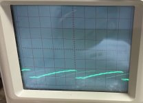
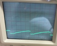
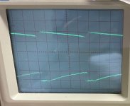
Here are some traces of what I see on the RAM data lines. Are they normal? I would have expected to see more transitions. Voltage scale is 5V/div and I don't recall the time scale.

IMG_7202.jpg
IMG_7205.jpg
IMG_7203.jpg
 
Even at 5V/div and no timebase information - they do look suspect to me on first glance...

I would suggest having a look at pins 1 and 19 of the RAM data bus buffers I10 and I11.

These pins control the direction of the data bus buffers between the RAM and the buffered data bus.

The buffered data bus is (in turn) buffered by E9 and E10 and controlled by pins 1 and 19 there as well.

Dave
 
At 1V/div those traces are even more suspect...

We need to ‘poke around’ the databus buffers first...

Dave
 
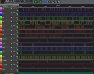
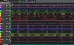
I spent some time beeping out connections and testing logic chips in my TL866II EPROM burner and haven't found anything broken. I also hooked up my logic analyzer to some of the main signals controlling the RAM. Here is an image of some output from that while the PETTESTER is running.
ram_signals.PNG

My interpretation is that it looks like /RAS0, /CAS0 and /W seem to never happen to be low at the same time. If I understand the timing diagrams in the datasheet for the 4116 correctly, this would mean that nothing ever gets written to the RAM. Does that seem like a correct conclusion? If so, are there any suggestions where to look for the fault causing this?

Thanks,
Greg
 
With such a nice looking Logic Analyser... it would be nice to see.. RA1, RA2, RA3, RA4 and RA5 all found at H9. Also... Nice to see nCAS0 and nCAS1 and nRAS0 all together... (I assume you have verified -5, 5 and 12 at the sockets).
 
Hi Greg,

You need to be a little bit careful with what you are looking at on a scope / logic analyser. You need to know what is happening on the CPU at the time interval you are specifically viewing.

For example, my PETTESTER will be writing to (and then reading from) Page 0 RAM. At the same time, the CPU will be reading instructions. At the same time, the PETTESTER will be updating the screen with G/B characters.

At the same time, the PET will be performing a DRAM refresh.

Your logic analyser will be capturing all of these cycles and displaying them to you!

What you need to do now is to read the chapter on triggers.

If you want to see if /RAS0 and /CAS0 are low at the same time, set the analyser up to trigger on this condition. You will then be presented with this condition (and only this condition).

You could also trigger on the condition when the lower bank of RAM is selected and the CPU R/nW is 0. You can then monitor all of the lines around the PET circuit associated with the RAM MUX, DRAM chips themselves and the DRAM data buffers and associated control signals.

A bit of light reading for you tonight!

Dave
 
I don't have one of these to play with but... if I did... I would remove the 6502 (or hold it in reset) and observe if refresh is happening. My guess would be that H9 has an issue (or maybe H6 that feeds it). Absence of refresh but good buffers would explain the memory results shown before... i.e. read it once get one value, read it again get another. H9 traces would be interesting.
 
Dave,

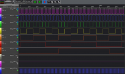
Thanks for the advice and impetus to learn more about my new toy, the logic analyzer. The results below indicate to me that the zero page of RAM is indeed getting written by your PETTESTER (or at, at least the control signals necessary for that to happen are present.)

RAM_writes_pettester_resised.jpg

Does anything here look unusual?

Greg


Hi Greg,

You need to be a little bit careful with what you are looking at on a scope / logic analyser. You need to know what is happening on the CPU at the time interval you are specifically viewing.

For example, my PETTESTER will be writing to (and then reading from) Page 0 RAM. At the same time, the CPU will be reading instructions. At the same time, the PETTESTER will be updating the screen with G/B characters.

At the same time, the PET will be performing a DRAM refresh.

Your logic analyser will be capturing all of these cycles and displaying them to you!

What you need to do now is to read the chapter on triggers.

If you want to see if /RAS0 and /CAS0 are low at the same time, set the analyser up to trigger on this condition. You will then be presented with this condition (and only this condition).

You could also trigger on the condition when the lower bank of RAM is selected and the CPU R/nW is 0. You can then monitor all of the lines around the PET circuit associated with the RAM MUX, DRAM chips themselves and the DRAM data buffers and associated control signals.

A bit of light reading for you tonight!

Dave
 
Nivag,

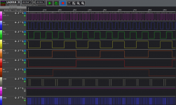
I followed your suggestions and looked at the refresh counters. Initially I was having trouble getting the signals off H9 because that was one of the few chips I hadn't already had to replace and the solder and chip legs were too oxidized/corroded to get good contact with a scope probe or logic analyzer clip. I finally decided to just pull the chip off, clean up the corrosion in that area, and put in a new socket and chip. A new chip at H9 didn't change the behavior. So I proceed to take some traces of the refresh signals with the logic analyzer, with and without the CPU in place.

Without the CPU:
refresh_counters_nocpu_resized.png

With the CPU:
refresh_counters_cpu_resized.png

So, it looks like the counters are counting, so that's good. One observation is that /CAS1 is always high, which I think is due to this being a 16k machine with the memory in one row (I know CAS isn't directly involved in refresh, I just hooked them up to see how they related.) The other observation is that RA7 has a phase shift of 1/8 of its period (pi/4 or 45 degrees) with respect to the other bits of the refresh counter. I'm not sure if that's significant or unexpected, but it was something I found unusual. Perhaps this is due to that bit being produced at H11.

In any case it looks like lots of things are working, at least at the chips producing the counters. Where would you go looking now?

Again, thanks for your help,
Greg
 
Those traces look fine to me (on a quick check at least).

As you can see, triggers are the all important factor with both an oscilloscope and a logic analyser. If you suspect that a write is not occurring, set a trigger up to look for the presence of the signal combination for a write. If it doesn’t trigger - either you have setup the trigger incorrectly, or one isn’t happening. If it triggers - and investigation subsequently indicates it is valid - then one did occur.

I would go back to the data bus buffers next. First look at the control signals for the data bus buffers (don’t forget there are the buffers from the DRAM chips to the buffered data bus and then the buffers from the buffered data bus to the CPU data bus (if memory serves me correctly).

The next thing to look at is the data bus signals themselves (these were what looked terrible a few posts ago). I would like to rule out the data bus buffer control signals first (you had a few above and they looked OK). What we are then left with is the bus buffer ICs themselves or the DRAM chips.

Make sure you put R/nW and /CAS0 on the traces.

If my PETTESTER is running the initial page 0 memory test (and it is failing) it will be cycling around on page 0 - hence only /CAS0 will be operational (memory containing page 0) and not /CAS1.

Dave
 
Those are nice refresh traces. Do you see them making their way all the way to the DRAMs themselves (i.e. through the muxs)? (And you are 101% sure the voltages for all rails are good at the DRAMs)
 
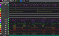
I looked at the refresh signals on the address muxes tonight. On the muxes themselves I connected the logic analyzer to the 7 refresh bits, the two mux control bits, and the 7 output bits for the RAM address. Here's some output:
refresh_counters_RAM_address_at_muxes.PNG

The output is a little fussy to interpret. My understanding is that the output of the muxes should follow the refresh inputs whenever CLK1 is low. My method was to first set up the logic analyzer to trigger when all of the refresh address bits were low and when CLK1 was low. I verified that the all the corresponding outputs were low. Then, I toggled the trigger for a single refresh bit so it was high and verified that the corresponding output bit was the only bit that was high when CLK1 was low. I repeated this for all 7 bits. Then I randomly checked several different refresh bit configurations when CLK1 was low and found that the outputs were the same as the corresponding inputs. So, it looks like the refresh counters get to the output of the muxes when expected. One thing that confused me for a while is that RA7 goes to FA0 and then RA1 goes to FA1, RA2 goes to FA2, and so on.

I made sure that the resistance between the mux outputs and the RAM address inputs was about 68 ohms for all 7 resistors that carry the address signals. In addition I double-checked the continuity of the address lines between the individual RAM chips. I haven't looked at the refresh signals on the RAM itself yet.

I also confirmed the supply voltages at each of the RAM chips: 4.97 V at pin 9, 12.17 V at pin 8, -5.06 V at pin 1. So those look good.

It's looking more and more like the refresh addresses get to the RAM chips. I'll check the addresses on the RAM chips themselves next.

Maybe it's possible that there is a timing issue that the refresh address aren't correct when /RAS0 is low, /CAS0 is high and /W is high? That seems like it should be a improbable fault.

After this I guess I can use the same technique I tried here to confirm that the data addresses through the multiplexers follow the inputs for the row and column addresses. And then there's the data lines and buffers to check as well, as per Dave's post above.

Cheers,
Greg

Those are nice refresh traces. Do you see them making their way all the way to the DRAMs themselves (i.e. through the muxs)? (And you are 101% sure the voltages for all rails are good at the DRAMs)
 
Back
Top