• Please review our updated Terms and Rules here

Memory problem with PET 2001

It's easier to see with no CPU. You should just get FA0...FA6 incrementing and nRAS toggling at 2x; that should be enough for refresh. Everything looks fine so far... which is why I keep mentioning voltages...
 
Post #28 should cover the rail voltages.

Worth double-checking them though with an oscilloscope - looking for dc level and ripple/noise.

That should put the rail voltage issue to be fairly quickly.

Can we then look at the data bus in more detail please please?

Dave
 
I suppose it is also worth pointing out that there are two (2) +5V regulators (and, therefore, two +5V rails) on the PET 2001N.

Obviously, both dc supplies need to be within tolerance for the PET to function correctly...

Dave
 
It's easier to see with no CPU. You should just get FA0...FA6 incrementing and nRAS toggling at 2x; that should be enough for refresh. Everything looks fine so far... which is why I keep mentioning voltages...

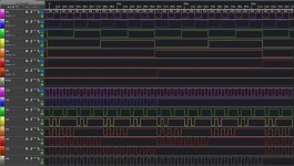
I pulled the CPU as you suggested and get exactly what you describe:
refresh_counters_RAM_address_at_muxes_nocpu.jpg

I also looked at the RAM supply voltages again, which I'll cover in a post below.

Greg
 
Post #28 should cover the rail voltages.

Worth double-checking them though with an oscilloscope - looking for dc level and ripple/noise.

That should put the rail voltage issue to be fairly quickly.

Can we then look at the data bus in more detail please please?

Dave
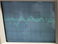

I checked the voltages at the RAM chips again and looked at them on the scope. The results are below. All scope traces were taken AC coupled at 20 mV/division

pin 9, 5V: 4.97 V
5V at DRAM.jpg

pin 8, 12V: 12.17 V
12V at DRAM.jpg

pin 1, -5V: -5.06 V
-5V at DRAM.jpg

These were taken with the PETTESTER running. Whenever the screen changes (about every second) the details of these waveforms "jumps" but then settles back down. I neglected to measure 5V at the processor end of the board, which I think is what the other regulator drives. It's hard to know which handles what without following the traces.

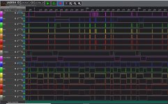
I also looked at the data lines at the buffers near the RAM chips (I10 and I11) with the logic analyzer. An image of the waveforms is below. I only have 16 channels so I'm showing the 7 lowest bits and the two control signals. The high order bit seems to behave pretty similarly, though.
RAM_buffers.jpg

Again, it's a little hard to totally understand this, but by setting the triggers for the data lines on each side of the buffers to the same bit pattern and looking at the signals when the LO READ and LO WRITE signal are low, I think that the signals are the same on both sides of the buffers when they're supposed to be. I think this means that the buffers themselves are probably ok.

However, there are a bunch of correlated "glitches" on the data lines on the DRAM side of the buffers, all or most of the data lines spuriously going high at the same time when they're not attached to the data bus. This can also happen during a read, which the buffer seems to propagate back across to the rest of the buffered data bus. When writing, the buffers seem to be able to pull those signals to the correct value and the values on the DRAM side of the buffers follow the input values. There are also often transients in the LO READ signal when it should be low.

My thinking is that these inconsistent signals are the next step up the chain of causality as to why the RAM isn't working properly. Are there any ideas as to what could be causing this? I wish I had a digital scope so I could try to capture these transients in more detail than just with the logic analyzer. Maybe that should be my next purchase.

Again, thanks for all the help so far and for any more help you can offer.

Greg
 
Last edited:
If you plot FA0...FA6 and nRAS (and maybe a few more for good luck) at the DRAMs when there is NO CPU present you should get clear refresh signals on that side. That would eliminate most things.

Also... Have you depopulated the DRAM? Maybe going to a small number of devices would help if they are contending with each other?
 
Assuming RDx is the RAM Data, then the logic analyser is indicating potential problems somewhere...

Unfortunately, a logic analyser is no good for looking for this type of potential fault. You need to use a scope.

Can I suggest doing what is in post #47 and I will think about how to proceed on the data bus?

What make and model is your scope? I will see if we can interconnect your logic analyser and scope together...

Are any if your DRAM chips in sockets by any chance?

Dave
 
I'm sorry I only just understood your plot...

The only times that really matter are when LO_READ or LO_WRITE are low. (It's nice to see that LO_READ and LO_WRITE are mutally exclusive!)

Now when LO_READ is low this means read from DRAM... RD0 and friends are not positively driving... bad news... and on the other side of the buffers it is doing its best but it's glitchy because of the DRAM side. The 74LS244s are schmitt triggered and you can see this as they square up the incoming glitch.

When LO_WRITE is low the CPU drives... and you see this happening.

I think that proves the buffer on the plot is fine and that LO_READ and LO_WRITE are good.

It does however show the the DRAM isn't driving.

That's my 2c anyway.

PS

I see on an earlier trace that MUXA is flat. That's not good. MUXA is needed to select the row/col.

If MUXA is always low... look at pins of H4.
 
Last edited:
I ordered a digital scope, a Siglent SDS1202X-E, https://www.amazon.com/gp/product/B06XZML6RD/ref=ppx_yo_dt_b_asin_title_o01_s00?ie=UTF8&psc=1 and it should be here tomorrow. My current scope is a cheap 20 MHz analog CRT scope that I literally found on the side of the road with a "Free-works" sign on it when I was working Palo Alto. Silicon Valley, man. It's pretty useless for looking at transients, but has served me well until now.

I socketed all the DRAM and swapped around the chips a bunch because, well, it was something I knew how to do and thought maybe it might help. Obviously it hasn't, but yes it's easy to pull a chip for troubleshooting now.

I'll try some of the above suggestions this weekend.

Cheers,
Greg

Assuming RDx is the RAM Data, then the logic analyser is indicating potential problems somewhere...

Unfortunately, a logic analyser is no good for looking for this type of potential fault. You need to use a scope.

Can I suggest doing what is in post #47 and I will think about how to proceed on the data bus?

What make and model is your scope? I will see if we can interconnect your logic analyser and scope together...

Are any if your DRAM chips in sockets by any chance?

Dave
 
When I first started troubleshooting this the problem was intermittent and seemed like tilting the board one way or another would cause it to start up seeing the full complement of memory, which makes me suspect a bad solder joint or other poor connection somewhere.
I'm starting to think that functionally all the bits are working... and that it is a poor connection. To enable the DRAM you a need a nRAS, nCAS, nWE and the respective supply voltages... all these signals have examples that look correct on the earlier plots. I've run out of suggestions and will stand back for a bit.
 
I spent some quality time with my new storage scope looking at stuff and I think everything I see with respect to the RAM seems plausibly correct.

For example, here is the refresh signal for address bit FA4 (yellow) and /RAS (blue) taken directly at a RAM socket, with no CPU and no RAM chip in place:
View attachment 66140

Here is the LO_READ (blue) signal at the DRAM buffers and a data bit on one of the RAM chips (yellow)
View attachment 66141
It looks like during the read the DRAM is trying to pull the signal high or low. This seems plausible. I neglected to grab an image, but it also appears that the corresponding line on the buffered data bus side of the 74LS244 also gets pulled high/low at the same time.

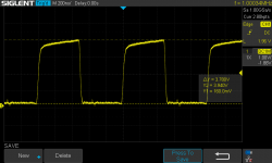
One thing that I was looking at that I'm somewhat concerned about is the 16 MHz clock generation subsystem. At the output of the 74S04 inverters (IC I1, pin4) I see the following waveform:
View attachment 66142
I had expected this to be more square-wavy and higher in amplitude. I had looked at this before with my 20 MHz analog scope, but assumed it was my scope bandwidth causing the weird waveform. Now, with a 200 MHz scope and probe I'm somewhat confident that this is a physical result. Is this an acceptable waveform?

Next, I expected the 74LS08 AND gate at G1 to clean the signal up somewhat. But, this is what I get out at G1, pin 6:
View attachment 66143
which doesn't look any better.

The 16 MHz clock is divided by 16 to produce the 1 MHz system clock CLK1 by the counter at G5. The output at its pin 7 looks like this
G5-7.png
So, now a more plausible clock waveform, but not great.

The 16 MHz clock is also used with the shift register at H3 to produce 1 MHz clocks with different phase shifts. Could a poor 16 MHz clock input to the shift register cause a lot of clock skew and timing issues? The output of the one of the phases of the shift register (H3 pin 3) looks like
H3-3.png
Basically the same as the CLK1.

So I'm wondering if the clock circuit is bad and, if so, what's a good way to diagnose/repair it? Start replacing things from the oscillator out? I tried a different inverter for I1, but I only had a 74LS04 not 74S04 and the circuit stopped working completely, which isn't surprising in retrospect. I ordered some 74S04s.

I also accept that this could easily just be a poor connection somewhere. I have tried to beep out everything I can think of with a meter and fixed the only definitively broken trace I could find, so it seems like it must be an intermittent (but frequent) fault. Can anyone suggest a good strategy to find a fault like this? Should I go through and systematically jumper connections and note changes in behavior?

Again thanks for everyone's helpful suggestions,
Greg

I'm starting to think that functionally all the bits are working... and that it is a poor connection. To enable the DRAM you a need a nRAS, nCAS, nWE and the respective supply voltages... all these signals have examples that look correct on the earlier plots. I've run out of suggestions and will stand back for a bit.
 
Last edited:
The oscillator is fine. It’s a horrid circuit anyway...

Do you have facilities for programming a 2716 EPROM at all? I suspect what you require is a test program to read and write a value to (say) memory location 0.

Dave
 
Yes, I have a burner and 2716s on hand. I don’t know much 6502 assembly but I have an interest to learn and some experience with other instruction sets, so I can probably figure out something out fairly quickly. Or do you have code you can share?

Thanks,
Greg

The oscillator is fine. It’s a horrid circuit anyway...

Do you have facilities for programming a 2716 EPROM at all? I suspect what you require is a test program to read and write a value to (say) memory location 0.

Dave
 
Excellent.

You're awake early!

I assume you are using BASIC4? It matters as the entry point into the EDIT ROM is different for each version of BASIC. I am at work at the moment and I have a meeting in a few minutes so no time to check the posts...

Dave
 
Can anyone suggest a good strategy to find a fault like this?
I think they are writing, not reading but all the RAS/CAS etc are OK. Now they would only WRITE not READ if you had a short to ground on nWE... so if I was looking for dodgy connections it would be nWE i.e. the Pin 3s is where I would start.
I think you said in Post#1 that the behaviour changes if you tilt or flex the board? Does it still do this?
 
I am between meetings at the moment. Assuming BASIC4 (and a non-CRTC machine) - here is a simple test program:

Source:

Code:
    ORG $E000   ; EDIT ROM for BASIC 4 (no CRTC).
    
LOOPY:

    LDA #$00    ; Load A with 0
    STA 0       ; Store A to address $0000
    LDA 0       ; Load A from address $0000
    LDA #$FF    ; Load A with FF
    STA 0       ; Store A to address $0000
    LDA 0       ; Load A from address $0000 
    JMP LOOPY   ; Keep repeating...
    
    END         ; End of test program.

Listing file:

Code:
E000                          .ORG   $E000   ; EDIT ROM for BASIC 4.
E000                LOOPY:       
E000   A9 00                  LDA   #$00   ; Load A with 0
E002   85 00                  STA   0   ; Store A to address $0000
E004   A5 00                  LDA   0   ; Load A from address $0000
E006   A9 FF                  LDA   #$FF   ; Load A with FF
E008   85 00                  STA   0   ; Store A to address $0000
E00A   A5 00                  LDA   0   ; Load A from address $0000
E00C   4C 00 E0               JMP   LOOPY   ; Keep repeating...
E00F                          END      ; End of test program.

LOOPY:              E000 DEFINED AT LINE 4
                    > USED AT LINE 12

Program the HEX bytes into a 2716 and put it in place of the EDIT ROM.

Incidentally, there is a very nice online assembler at asm80.com. Despite the name, it will assemble 6502 code! It will also produce a HEX (or BIN) file directly for loading into an EPROM programmer.

The test program first writes $00 to memory address $0000 and then reads memory address $0000 back again. It then repeats this with the value $FF - and keeps on doing this forever. You can change the data patterns it reads and writes by modifying the bytes at ROM offsets $0001 and $0007.

You should be able to look in much more detail at the RAM read and write cycles now (we are only playing with one address at $0000) and you should be able to see the exact data that is being read and written.

Might be worth waiting for dave_m to check my simple program first - he usually finds some fault or other with them :)! Unless you want to take a flyer...

Dave
 
Daver,
I like to play 'junior coder' with your test routines. I always learn something. I noticed you used the zero page instructions with the LOAD and STORE Memory instructions instead of the absolute memory instructions. Saving space!
 
Back
Top