• Please review our updated Terms and Rules here

Neglected PET needing some love

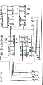
Oh man that took a really long time but the new ram chips finally came in. I replaced UA4 with one of the 8116's. The pattern pettester is giving me looks the same though:

20221128_145833.jpg

For reference here was what it looked like using the original chip in UA4:
ramBanksSwapped.jpg

I still expected some bads but not in the same place. I guess I could go ahead and just install sockets for all of the 2nd bank chips, or just take them one at a time.
 
So, just to refresh my memory...

We originally had my PETTESTER working ok with the /CASx lines around the other way around. Yes?

All you have done is to swap the two banks of 16K RAM over. Yes?

Dave
 
I have just checked my own posts back in 243 and 245 and already identified data bit 0 (UA4) was stuck low, data bit 1 (UA6) was stuck high and data bit 5 (UA14) was potentially stuck low.

Looking at the first 4 memory cells, I don't think you will see much change unless you change both UA4 (which you have done now) and UA6.

With faulty D1 and D0:
00 10 b
01 10 b
10 10 g
11 10 b

With faulty D1 and good D0:
00 10 b
01 11 b
10 10 g
11 11 g

There should have been an observed difference in the 11 case, unless another data bit was faulty that was messing with us!

Dave
 
Last edited:
I have just checked my own posts back in 243 and 245 and already identified data bit 0 (UA4) was stuck low, data bit 1 (UA6) was stuck high and data bit 5 (UA14) was potentially stuck low.

Looking at the first 4 memory cells, I don't think you will see much change unless you change both UA4 (which you have done now) and UA6.

Dave
Alrighty I'll desolder and socket UA6 the next time I get some time to work on it. Probably will have to do it to UA14 as well, maybe more.
 
Possibly, but let's take them one at a time shall we...

It can't be anything else (address multiplexers or data buffers) as these are all common to both banks of 16K. If everything is working fine on one bank, but not the other bank, it is either a high address line issue or the DRAM chips itself.

It is strange that replacing D0 by itself didn't have much effect, but I can see a slight change in the pattern when it is actually removed.

I'll have another quick look tomorrow when I am not on my phone.

Dave
 
Last edited:
I was just having a look at the results, and I worked out that D0 and D1 are bad as well. When @daver2 mentioned UA4 and UA6, I wonder if you meant UA16 (bit 0) and UA14 (bit 1).

This might explain why you didn't see any change when removing UA4.

For reference, I'm looking at this schematic.
 
You may have missed a key post back in #284.

Originally, this PET was working OK with the lower bank of 16K - but the upper bank of 16K was not working.

We swapped around the two (2) banks of 16K by swapping the /CASx lines over to put the faulty (upper) 16K of RAM into the lower 16K of memory space.

The thread then disappeared into a keyboard repair whilst waiting for some replacement DRAM to arrive in the post.

Therefore, you have to imaginarily swap over the two banks of DRAM on the schematic in your mind...

Effectively (with the wiring modification) UA4 has become D0 of the lower 16K bank of RAM and UA5 has become D0 of the upper 16K bank of RAM.

Dave
 
Last edited:
Sorry, I did make a mistake. I meant to say I would still suspect UA18 (not UA16) and UA16 (not UA14).

Swapping the CAS lines wouldn't change the data lines would it?

(excuse the poor drawing)

EDIT - sorry just saw your last sentence.
 

Attachments

  • ram.png
    ram.png
    54.6 KB · Views: 8
Hmmm,

That's interesting, so we may have inadvertently swapped a GOOD Data Bit 7 over and not a FAULTY Data Bit 0... Doooo!

Perhaps we ought to double-check and confirm what machine this actually is and which schematics apply before moving on further...

Good catch.

I have just gone back through the thread - and I made the error much earlier on...

Dave
 
Last edited:
I wonder if piggy backing UA18 or UA16 will make a difference in the results from pettester? I know it's not the most scientific way of diagnosing issues, but in some cases it might work...
 
For a DRAM that is suspected as pulling the data line LOW (D0) then the piggyback method is unlikely to work. However, for D1 - where I suspect the data line is being pulled HIGH, then the piggyback method may work. There is still some science to the piggyback method...

Dave
 
Well that took a lot longer than I thought. I got hit with covid and it's been kicking my ass. At one point I felt semi-okay so I decided to try desoldering UA18 and UA16 to add sockets only when I finished I realized I screwed up and did UA19 and UA17 instead. Doh. That's what I get for trying to work on electronics when I'm sick as a dog and not thinking straight.

Anyway I finally managed to get 18 and 16 replaced and the results are promising but still issues. I decided to upload a video this time instead of a still because there's some characters that are switching on the fly and at least one "g" sometimes turns "b" This was probably happening all along.

 
My wife went down with it. She was knocked for six for a couple of weeks. I caught it from her but had minimal effects. I think it's just the luck of the draw I am afraid. Glad to hear you are on the mend though.

Ignoring the strange and weird effects - I see a block of 32g followed by 32b. In binary: XX000000 through XX011111 are 'good' with XX100000 through XX111111 as 'bad'. I suspect Data line 5 (D5) as being duff (output held LOW). This would equate to IC UA8 (with the upper bank being swapped around for the lower bank).

I suspected D5 back in post #243 (but screwed up my IC identification there by getting the data bits numbered backwards for some reason).

Can someone please check my logic before @Divarin starts work?

Time to warm up the soldering iron again (or hasn't it gone cold from the last time?).

This is the best way - is to look for obvious 'power-of-two' blocks of good and bad and then work from there.

Dave
 
It is worth reviewing pages 11 and 12 of this article which explains the way the DRAM chips can misbehave when they fail. This helps to correctly interpret the results of DRAM testing (however it is done). There are essentially 4 ways they can fail which you need to be aware of and they can also create an apparent intermittent abnormality too as explained there. If you are not ready for that variation, it can create some confusion interpreting the defective data and isolating the correct IC. Beyond page 12 there a 5 types of failure examples to illustrate the main points:

 
That did it! No more bad ram, it looks like. The test continued on to the keyboard test and after that countdown continued to the comprehensive ram test. 1 pass so far I'll let it run for an hour or so.
 
Excellent work...

Let it run for a while and then revert the /CASx wiring back again so that the 16K banks are the correct way round once again.

We then need to see whether PETTESTER can successfully see (and test) the full 32K - or whether replacing RAMs that we needn't have done has introduced some problems again...

Dave
 
Back
Top