However... I've noticed something strange as I looked at my motherboard. Pins 2 and 14 should be connected on ALL RAM chips! Mine doesn't have that! I'm not sure if it would make a difference, but I'd like to try, at least.
AAAAAGH! Do not do that. It will make no difference and depending on what's different about what Sanyo did you may well break something. Pins 2 and 14 are the "Data in" and "Data out" pins on that style of memory chip. If the Sanyo doesn't have them tied together across banks it might be doing something differently than the 515x, like using a separate data buffer per bank instead of one for all four. If the machine is working now it's working as intended, and this will have *absolutely no effect* on how memory is addressed. You'll just be shorting stuff together that for some reason Sanyo decided to separate, and possibly putting adverse loads on the non-enabled banks when the active one is trying to respond.
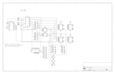
So, from what you're telling me, since the 24S10 is central to all this, in relation to the RAM decoding ICs (the 138s), I should be looking at the RAM ADDR SEL line, then.
YES. This is what I've been repeating for several posts, and I really tried to make it clear in
this one, but let's try again.
An 8088 has 20 address lines, which all together can count in binary from zero to 2^20th, or a little over a million in decimal. IE, one megabyte. Your computer divides this possible total address space into chunks which are assigned to different functions, like RAM, ROM, video memory, whatever. All of these devices sit in parallel on the data bus, IE, the same data lines run to all of them, and they would all be shouting at the same time and stepping on each other if it wasn't for address decoder circuits to decide what was active and what wasn't depending on what address the CPU is asserting on the address bus.
RAM in a PC compatible starts at address HEX x00000h and runs in a contiguous block up to as high as x9FFFF. (640K) IE, out of the 16 possible 64K sections that fit in 1024K the first 10 are candidates to have RAM in them. Here is how a 256K IBM 5150, which does not have a PROM doing the job, sorts out how to assign each of four 64K banks of memory chips to one of four slots in the first 256K of the total address space:

A18 and A19, which are the top two address lines, highlighted in
BLUE. With their 2 bits you can therefore choose one of four 256K slices of address space, which we will call pages zero through three. They connected to an LS138 multiplexer in such a way that the only used output line, which is "RAMADDRSEL" in this example, will be active low when "PAGE0" is active, IE, the CPU (or a DMA-driving peripheral) is looking to read or write the first 256K of address space, and inactive (high) all the rest of the time. This line, which I highlighted in
GREEN, is used directly to drive the chip enable of a 74245 buffer that sits in front of all four banks of RAM, and it is *also* used as one of the enable lines for the LS138s that generate RAS/CAS signals; this is what gates ALL the RAM chips from trying to do read/write cycles when they're not being addressed.
Now look at the lines highlighted in
RED. These directly connect A16 and A17 to the RAS/CAS multiplexers. A16/A17 again together give four possible selections, this time letting you choose one of four 64K blocks out of a total 256K range. The LS138s directly break that two bit number into the four RAS/CAS signals; since all RAM banks are the same size you don't need to do anything more elaborate than this, mapping directly to the address lines works. And that's basically it.
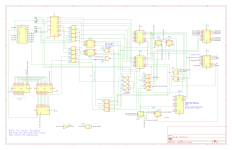
So let's see why the 5160 uses that PROM:

On this system we have the 24S10 PROM in place of that 74LS138 in the 5150. This time the address lines, again highlighted in
BLUE, which run to it include all four of A16-A19 instead of being split. The reason for this is because now we have the possibility of RAM banks being different sizes; instead of just being able to conveniently assign the same power-of-two granularity to all four banks you want two of them to be enabled according to this truth table:
| A19 | A18 | A17 | A16 | Bank # (decimal) |
| 0 | 0 | don't care | don't care | 0 |
| 0 | 1 | don't care | don't care | 1 |
IE, bank 0 needs to be active for all of the first 256K page and bank1 active for the second 256 page, while the other two need to follow this:
| A19 | A18 | A17 | A16 | Bank # (decimal) |
| 1 | 0 | 0 | 0 | 2 |
| 1 | 0 | 0 | 1 | 3 |
IE, when we're between 512K and 640K, A19-A17= 100, we want one of two 64K banks selected. In other words, we want an asymmetric equation to apply to what gets asserted on the
RED lines which run to the CAS/RAS 138s. And, also, of course, we want that
GREEN ADDRESEL line to be active when any of the banks are supposed to be active, IE, for the entirety of the bottom 640K block of RAM. To be clear, you don't NEED to use a PROM or PAL or whatever to do this; give me a few minutes to think about it and I could hack you together a schematic to do it with LS138's and some AND gates, or just NAND gates, or whatever, there's a million possibilities. The PAL/PROM just makes it easier because it means just one part can hold a bunch of different possible memory maps which can be switched between based on jumpers/switches.
(IE, look at the PROM in the 5160: it has eight address lines, of which only four are connected to the computer's address bus. The other four are connected to switches and jumpers. That means that the machine can support 16 different possible memory maps for RAM. This would be really messy and annoying to implement in discrete logic.)
That you're tossing out things like "maybe pins 2 and 14 on the RAM chips not being tied together" is the problem really makes me feel like you're not groking the basic concepts here.
 On the clone schematics, I see LS00 chips in place of where the PROM would go. (The university paper tells me that there's a RAM decoding CIRCUIT, and a PROM Decoder [for those who managed to clone that too], which holds the logic for the memory map, in XT computers.)
.png")
 3.png")
 2.png")