Hugo Holden
Veteran Member
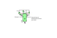
Hi Antony,hi guys, @daver2 @Hugo Holden I have completed the new drawing and I would like you to check if everything is ok.
I drew without tags because I noticed you don't like them.
please report any errors because I'm learning, thanks.
If it helps but I discovered an error with the monitor connector on the previous PCB.
There have been so many changes to the wiring, I have lost track of what is connected where and on the prototype board that Desperado is trying to fix.
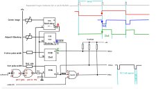
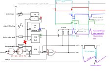
The main thing at the moment, is to go back to basics and how it is supposed to work. See attached timing diagram.
One improvement I think would be to trigger monostable IC2A from pin 8 of the 74LS10, rather than the collector of Q1 directly, because it is a better compatible TTL rise & fall time at that point after being squared up by the two gates and monos can be tricky with triggering.
Ideally the monostable IC3B that generates the the H drive pulse should not be adjustable, and simply set close to 23uS with a fixed resistor and timing capacitor.
Likewise IC3A for the vertical pulse is better settled on a fixed value close enough to 1.26mS
The one H line delay (63uS) needs to be adjustable to center the video text, and the 10uS H blanking pulse adjustable in case the 10uS wasn't quite long enough to blank the H retrace in the VDU.
I haven't draw in the capacitor values or preset values, but the capacitors were already settled on and the presets chosen.
So perhaps if you could re-draw up the new schematic to conform to this basic arrangement and check the timing values from the IC data sheets, it should work.


