• Please review our updated Terms and Rules here

C64 IN PET S' CASE

Do you mean JP7 or J2? It is J2 on the PCB is it not?

Do not bother about J2 until you have sorted JP1 out.

Do NOT connect J2 to anything in the meantime...

If the schematic shows pin 1 of JP1 is +5V, but the PCB has pin 1 of JP1 as GND - then there is an inconsistency between the schematic library footprint and the PCB footprint.

Please note all of these issues down in a NOTEBOOK. You will need to provide a list of these errors to anyone building your board - or to correct the next iteration.

Dave
 
By the looks of the PCB, J2 pin 1 goes to diode D3 and to IC1 pin 8.

Ah, it looks like pin 1 of the ICs (the 'square' pin) is also not pin 1of the IC...

Dave
 
I can't tell from the photograph you posted...

Can you post a sharp photograph of the top and bottom of the PCB.

Dave
 
Top
And bottom
 

Attachments

  • 1702224601423..jpg
    1702224601423..jpg
    1.5 MB · Views: 13
  • 1702224694752..jpg
    1702224694752..jpg
    1.3 MB · Views: 13
It looks like J2 pin 7 is 0V/GND. J2 pin 7 should have a thermal relief pad to the ground plane.

It also looks to me as though there are solder splashes on the board, and it also looks like that some of the solder joints may be shorting out to the ground plane. if this is the case, you need to fix issues these FIRST.

Ground planes are great for reducing electrical noise and cross-talk - but they require much more care in construction to prevent accidental short circuits.

Dave
 
Guys, I looked at the first PCB and this j1 is the same, I made a mistake in writing the silk-screen numbering. however there is an error in j1 in the footprint which is upside down but it wasn't a problem in the previous PCB.
The J2 connector is correct, in the past I thought it was a mistake but looking closer I realized it was correct.
the chip footprints are correct, I checked them again and verified they are the same as the previous PCB with the replacement of 74LS08 with 74ls10. The TTL chips are robust and withstand polarity reversal but I can't be 100% sure, in my opinion you have to check everything.
 
I placed the wires on the jp1 connector, now with the oscilloscope I have the video signal on pin 1 of J2 but I don't see the horizontal and vertical signals on pins 3 and 5 :(
 
Did you expect to?

I told you ages ago that it wouldn't work first time didn't I...

Have you adjusted the potentiometers or not?

Start at the input signal from the C64 and work through the synchronisation logic a step at a time with your oscilloscope...

Dave
 
>>> Not again...

Well, how are the potentiometers going to adjust themselves, by magic!

>>> I have a waveform on the video signal coming from the c64 but I don't know if it is correct

Well, we measured this signal time and time again in this thread. So go back over the posts until you find it, and then compare what it was then to how it is now.

You have a trace already in this thread of most of the signals that you should be getting.

Dave
 
If the 4 IC's on the board got exposed to reverse polarity and the current was enough to blow the fuse, likely the chips are damaged. But I don't know if that happened or if the +5V supply just got shorted out.

I would drop in a new set of IC's, put those ones aside for now, Later, when the board is working, you can substitute them back in, one by one, and find out if any of them still work.

Question for @daver2:

Do you know where we could see or get a scope recording of the video signal that comes out of the C64 computer, specifically in the vertical sync area ? We could ask Desperado to try to record one on his scope, but it can be difficult with a scope not designed to lock to vertical sync and without a delay timebase, like the V509 scope for example. Maybe it was documented in the manual ?
 
Last edited:
Hi Hugo.

Somewhere in the 1,537 posts of this thread we did take a trace of the input to the new video board (which is the same point as the output from the C64).

I have given Desperado the job of searching for the requisite image because I am too busy at the moment.

EDIT: OK, I found a couple:

Post #532 on page #27 of the thread.

Post #653 on page #33 of the thread.

One is better (height wise) than the other - but the oscilloscope is not synchronised to the signal so it has a few ghosts...

Dave

Dave, those Oscillograms show line rate recordings. We need to see a signal in the vertical sync interval to show at least 5 or 10 lines or so around the vertical sync.

One problem in this whole project is that we never got to see the way the H sync pulses behaved during the vertical interval in the C64 signal.

If it was just standard NTSC style , but monochrome video, I could guess, but in Computers they did all sorts of things to it, knowing that the VDU's scan oscillators would gloss over it.

Clearly the C64 was designed to feed a style of VDU that had independent scan oscillators, and these are very very forgiving. They don't care if the H sync pulse vanishes during the V sync pulse.

The thing is though, Desperado is trying to drive the 9" VDU that requires very specific drive waveforms to make it work.

Specifically, the H drive wave which requires a drive signal of the correct frequency and duty cycle and completely un-interrupted by any glitches in the vertical block. This is why he had that odd problem of the Bumble Bee buzz.

The original Commodore circuit we have been struggling with, was definitely designed to feed a VDU which had its own H scan oscillator and locked to the H sync pulse. (Unlike the unique 9" VDU). The PLL nature of the 12" VDU in the H scan oscillator, smoothed out any errors in the vertical sync interval.

But , he/we have tried to re-task the Commodore circuit for the 9" VDU. When, it might have been better to start with a different design concept for the task.

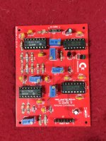
Still we may be able to get what he now has to work, as at least all the essential elements are now present on the board.

But I cannot make a lot of sense out of it unless I could see a conventionally drawn schematic and the actual video signal driving it in the vertical interval. Then I could predict what waveforms/signals should be present at each point on the circuit.
 
Hi Hugo, as soon as I get back from work I will post a current photo of the C64 output signal on the oscilloscope screen.
 
Back
Top