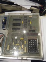
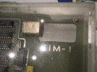
As promised, attached is a proper schematic for Brother Dwight's board. Having put some time and effort into it, I think I've earned the right to get up on my soapbox for a moment.
The schematic I worked from was apparently reverse-engineered from a PCB, as Dwight's original drawing was accidentally lost. The recreated schematic was, frankly, a mess - sketchy, inconsistent, and utterly failing to show any kind of rational signal flow. Signals entered in the middle of the drawing and from there went in all directions. Most of the connections weren't drawn at all, instead indicated by tags. The result was that it took an unusual amount of staring at it to figure out what was going on - in a simple circuit that anyone should be able to fully comprehend at a glance. Far from being complete, the information contained therein was so inadequate that to sort it out I had to refer to the original KIM manual, photos of the completed assembly, and stray notes.
I don't entirely blame the person who did it; I've done enough reverse-engineering to know that it's a buttload of work, and the time and difficulty involved are probably an exponential function of the number of components and nets. But if you're not ready, willing, and able to do it right, don't bother. Aside from apparently lacking any sense of what a schematic should look like, said person was further hobbled by the use of KiCAD. Now, I've thought a lot about how best to describe KiCAD's schematic capture, unable to settle on whether it's goat sodomy or a dumpster fire. Upon consideration, though, I realized that such a choice wouldn't at all be fair, because it's actually goat sodomy in a dumpster fire, and about the worst tool I can imagine for reverse-engineering, which inevitably requires repeated rearrangement of the drawing in order to wrestle a random pile of symbols and wires into a rational and comprehensible drawing. This is because its schematic capture has no proper understanding of the actual meaning of connections and nets. When you make what you think is a connection, it really isn't one at all - it's a faux connection, nothing but two coincident points in space that hold no significance whatsoever for KiCAD until some time later when a netlist may be extracted. But it's a recipe for disaster because it doesn't maintain net connectivity, which means it doesn't maintain design integrity. So I'm not just blaming the draughtsman for a bad drawing, because unspeakably poor tools make producing a quality document difficult or impossible even for someone who knows what the finished product should look like. I'm on the record as saying that KiCAD is, overall, an admirable accomplishment, and its layout tools may be first-rate, but I'll never find that out for myself as long as its schematic capture - the design process's front end - isn't fit for polite company or the attention of grownups. When I explain the reality of KiCAD's schematic capture to real live EDA professionals, their jaws drop. Every single time.
Enough of that rant. This how the drawing should look, and it encompasses all of the information needed to construct the circuit. It shows two versions: What I understand to be Dwight's original, based on the above-described recreation; my modified version. Dwight did one thing that I don't like, and that's asking totem-pole TTL outputs to sink current for the LEDs. LSTTL isn't designed to sink more than 8mA, and you can't get much brightness out of most LEDs with that little current - I usually think more along the lines of 20mA. So I replaced his 7404 with a 7405 (and the necessary pullups), and since he had two spare inverters those became my LED drivers. Oh - I also added a power LED. That may seem trivial and unnecessary, but without it this pair of boards can be live on the bench without any visible indication of such.
Hope you find it useful, and if you happen to spot any errors please let me know so I can sort them out.
 !
!
