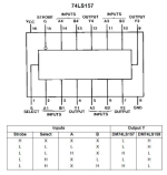
You need to break the truth table down into individual rows.
Each internal 'gate' (and there are four of them) have two inputs (labelled A and B) and one output (labelled Y). Delete the entire column for the '158 to save confusing yourself even more
")
!
If the STROBE (G) input on pin 15 is HIGH, the output (Y) is always LOW. The other inputs (A, B and SELECT) are irrelevant (hence the X - meaning "don't care").
If you look at the PET schematic (
http://www.zimmers.net/anonftp/pub/cbm/schematics/computers/pet/2001N/320349-7.gif) you should observe that the G pin (pin 15) is connected to 0V/GND/LOW - so the device is permanently ENABLED (and therefore the output Y always responds to the inputs A, B and SELECT).
With the SELECT pin (pin 1) LOW, the output (Y) responds to the A input.
With the SELECT pin (pin 1) HIGH, the output (Y) responds to the B input.
On the PET schematic, the SELECT pin (pin 1) is connected to CLK1 (which is a 1 MHz clock).
Therefore, when the clock is LOW, the Y outputs are connected to the A inputs and when the clock is HIGH, the Y outputs are connected to the B inputs.
For one half of the clock (LOW), the SAn signals are connected to the outputs from flip/flops and counters G6, F4 and F2 (A inputs to the '157).
For the other half of the clock (HIGH), the SAx signals are connected to the buffered address lines BAn (B inputs to the '157).
Can you follow my description with the logic table and pinout contained within the data sheet now?
As an exam question, can you work out what is wrong (from the datasheet pinout) on the PET schematic
http://www.zimmers.net/anonftp/pub/cbm/schematics/computers/pet/2001N/320349-7.gif for IC F3?
Dave