• Please review our updated Terms and Rules here

Honeywell 200 resurrection

Regarding tediousness, I would think that a language such as VHDL could also leverage building blocks, such that you simply use blocks to construct the machine.

I was envisioning a way to represent the original hardware logic, but using modern tools. I was looking at the "Series 200 Logic Training Manual" that I downloaded from bitsavers. That seems to describe the CPU logic in enough detail to (perhaps) reconstruct it, but the major diagrams are missing from the scan (or are part of a separate document bundle that is not available - or else I don't understand the references made).

I believe the same process (that you have been using) would be followed, except that instead of physical hardware one uses the language features of something like VHDL. (I keep using "VHDL" here because it is one hardware language I know of, but I suspect it is not the latest or best supported anymore).
Yes, to exactly replicate logical operation of the H200 you would need a complete set of flow charts as explained on pages 3-10 and 3-11 of the Logic Manual. A former field engineer might still have these but I doubt that they are really necessary as you should be able to guess most of their contents and you would only need them if you were keen to replicate every nuance of the original machine rather than just the specified behaviour of it as given in the operation descriptions. It all depends how genuine you want your emulation to be.

To understand my personal motivation you have to refer to my article written for the Computer Conservation Society here in the UK. There I explained that I just wanted to turn a big heap of electronic junk into a working machine so that I could give it away to someone else instead of having to pay for it to be recycled in an environmentally secure way as required by UK legislation. In the marketplace I think this activity is generally known as "value adding". By the way, that article isn't exactly as I wrote it as the editor of the magazine applied his own version of "value adding" to it without consulting me first. That's why I prefer to publish only on my own websites although that article gained me some interesting contacts.

I actually find the physical constraints of the project far more challenging than the logical ones. My design has to take into account a whole list of constraints that your approach probably wouldn't. Here are just some of them.

The limited number of pins on the very simple original ICs that I use.
The limited number of ICs that fit on one standard PCB.
The limited number of each type of IC that I have in my stockpile.
The cumulative propagation delays encountered in using chains of ICs.
The limited number of edge connector pins on each PCB.
The limited number of PCBs that will fit on one backplane.
The limited number of backplanes that I own.
Last and not least the appalling cost of getting integral edge connectors gold plated on new PCBs nowadays.

I am not acquainted with VHDL and don't know how all these constraints could be factored into a design while using it.

The appeal of the original H200 was that it was cleverly designed both up to a high specification and down to a low price. The economy exhibited in the logic design was impressive, which was probably why its chief designer, the late Dr. William L. Gordon, persistently described the machine as "elegant" to his family for the rest of his life according to his daughter. If you can work out the most elegant and economical way of designing the logic then that was most likely how the original design team did it if they were working to similar constraints.

If there were someone who would want to carry on with my project when I gave up on it then I would give them all the resources that I have for it but I doubt that such a person exists. I may still continue it to a logical end point to enable such a handover anyway if other commitments don't become more demanding just to find out whether what I have already designed actually works. The main memory is already operational and the control memory design still needs completion and proving, so I may go at least that far.
 
Lovely to see this forum. Sorry I won't be of much assistance, but oh wow the memories :)
I worked for Honeywell Information Systems in Brentford, London from 1970-1972 where we had a 48K H200 - 200 on the first floor and 132K (?) H1200 and 512K H3200 on the ground floor. I have been racking my brains out trying to remember the device numbers for the dis-mountable 10KB and 20KB disk packs - 259 and 272 spring to mind, but maybe that was IBM.
So 52.5 years later I'm still working with computers ( but not hardware now) - Been my job and my hobby all these years.
 
Ah yes, I think it was at the Brentford site that I was first trained in Easycoder programming in 1965 so I've known how to do that for a good few years now. I was never an employee there though.

I mentioned in an earlier post that I tend to turn my logical designs straight into PCB layouts without drawing schematics. I had some PCBs made up from one of these layouts back in 2019 but haven't got around to installing the components on them yet. Yesterday while deciding whether to resume my project I looked at the the layout and couldn't remember how I intended to use the boards as the design was as convoluted as my Easycoder programmes used to be to achieve the maximum possible in the smallest space. It's taken me a whole day to work out how the boards are meant to work. Perhaps I should have drawn some schematics ...

I don't want to waste the time that I've spent on the design so far, so I will probably build what I have already designed while I'm waiting to see whether my reticent friend in California does send the control panel. I have just sent him a letter as he seems to respond to letters even when he doesn't read or reply to emails. I can only wait and hope but mail from the UK to California takes a while and so does he.

By the way, last year I went off topic and mentioned that I had another project to occupy my time and now I have pretty much completed that, which is why I am contemplating starting work on the H200 one again. If anyone wants to explore the subject of that other project, the potential that a quantum neurobiological system (human brain maybe) might have, then visit my website MensTemporum.UK where I describe the weird coincidences that have occurred in my life when I have just acted without thinking rationally. Apparently creative thinking happens in a place where other strange things can also happen, such as the future influencing a person's present. This may well explain why I have always been irrationally optimistic about my H200 project, because at the back of my mind I may already know how it will turn out. The truth isn't out there; it's in here.
 
The only Honeywell 200 movie I've seen is Karl Malden in "Billion Dollar Brain". I had to get the BluRay so I could watch the whole scene. Quite instructive, as he actually does seem to be operating the H200. The opening titles do have some blunders in them.
 
Ya, there's definitely some Hollywood "special effects" in that movie. The printer with the voice output being just one of them. :D I have the DVD of the Billion Dollar Brain. I was talking to my dad tonight about the controls on the card reader (the one with the angled input deck) and that movie was the best place I knew to go look, although the text was a bit blurry (we figured it out). While searching for more info, I ran across that link about a film that Honeywell made of a few demos. The seller mentioned that they had converted the film to a video file and was going to supply it on DVD to the buyer, so there's a digital copy someplace. It would be cool to see it.

The scene in BDB where Karl mounts a tape is at least partially real. He does a correct boot from address 41 (the card reader), hits run and then the card reader starts reading in more cards. I did wonder if the walls of equipment in the background and the little plugboard he rewired were real or not...none of it looked familiar, although it could have been non-Honeywell equipment. The credits mention parts being shot at Honeywell labs somewhere, if memory serves.

On a related note, I bought a 16mm film by Honeywell for their 25th anniversary. One of these days I'll see about having it digitized and post it someplace. Maybe there's some H200/2000 clips in it.
 
I never did hear from that chap in California, so I am now looking into the feasibility of building a control panel from scratch again. I have enough switches, i.e. fifty, but not quite enough of the chunky buttons to fit them, so I will probably have to make those as well.

My wife and I just returned from a holiday trip during which we visited my acquaintance Marcel, who some years ago donated to my project the memory modules and driver boards that I used to build the main memory unit. He has now given me the rest of his collection of H200 components consisting of four more 4k memory modules and almost a hundred more logic boards. Although my memory unit only accommodates two memory modules I will now be able to select the two most reliable ones from the six that I have.

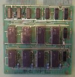
Of the other logic boards an interesting one is shown in this picture.

R3MAA.jpg

It contains eight 74181 four bit arithmetic processors, which suggests that it is configured for 32 bit arithmetic, but I don't know what kind of H200 it would have come from as the earlier machines in the 1960s used only transistors. I will ask my former Honeywell field engineer friend Brian whether he knows what it is and where it was used. Brian was the person who installed and maintained the first H200 bought by the company where I worked back in 1966, so we both well recall those days of punched card technology. There is a photo of the computer room where we both worked on my website although neither of us is in it.

A hindrance to analysing the board's circuit is that I can't find any information about the smaller support ICs. They have the Signetics logo on them and the numbers 7351, 7346 and 7338 and at first I thought that I had discovered some long lost 7300 series of ICs until I saw that the AMD 74181 ICs had 7346E on them and realised that these were the batch numbers! At least I now have an idea of the year when the board was manufactured. The actual type "numbers" on the Signetics ICs are DKVH1 and DKVH2 but I suspect that these may be custom ICs made specifically for Honeywell, in which case finding out what they do will be impossible except by testing them. However, if anyone can find out what they are I would very much like to know.

Apart from this occasional armchair research I am too busy with other things at present to resume construction of the machine but at least my plans are progressing in my head. I only had time to write this item while finishing off a lunchtime pot of tea. Actually this last cup of tea is almost cold, so I have evidently spent too much time on this already.
 
Yeah, I would interpret the 73xx numbers as date codes, so parts were manufactured in 1973. I'm guessing that the DKVH1/2 parts are bus drivers/multiplexers. You've got 3x32 lines for the 74181s, and 9x DKVH1/2, so both are a multiple of 3. Not sure how many pads connect to the bus on that board, but there must be some amount of sharing as you couldn't have 3x32 = 96 connections. Could this be from a H2000, or even a later model? I'm not sure how an H2000 would use that board, but an H8000 seems likely.
 
Thanks chaps. These boards are seriously restricted by having only single-sided edge connectors with just 36 contacts. That was fine when originally they each typically held maybe only four transistorised gates but ICs greatly increased the complexity of the logic that could be fitted on each one. It certainly makes designing circuits for them challenging. Bear in mind that they plug into a backplane rather than a bus so each has custom wiring to its contacts on the backplane. The only common bus connections are two ground connectors and the five volt supply leaving 33 other connections to play with. I'll trace the circuit and see what possible configurations there are, but maybe my friend Brian knows something.
 
That board is from the Honeywell 1100 option, also known as the "scientific unit". As I understand, it was basically a math co-processor for the CPU and was probably geared toward floating point in hardware. I remember begging my dad to let me have one because the 74181 was pricey for a young teen and I was learning TTL logic at the time.
 
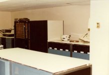
Here is a picture of the scientific unit attached to an H3200 system at my dad's warehouse. There are two tall cabinets in the back row. I think the one with the exposed backplane on the left is the 1100 and the other being the H3200 CPU (just a guess but I think the CPU would sit closer to the M9 memory to the right w/the numbered drawers, 64K/drawer x8 drawers = 512K, a lot at the time!)

BCS-H3200_Scientific_Unit.jpg
 
Last edited:
The floating point hardware I read about, for H200/H2000, used 48-bit representation (36-bit mantissa), since those machines are based on 6-bit "characters". So it's not clear to me how a 32-bit "ALU" would be used there. Seems like they need one more 74181. Unless they did something funky like carry over to another board. Not enough space on the PCB for 9x74181. But I guess we don't know yet how that board is wired - might not be one single 32-bit ALU. Even the 8200 series says it used 48-bit words for everything (40-bit mantissa FP).
 
I do recall there being more than one of these boards in an 1100A (the Honeywell options list refers to it as the 1100A), but I don't recall exactly how many. Bitsavers has some programming manuals for the 1100A if you're interested.
These couldn't have been wired in a "straightforward" 32-bit manner since you would need 2x 32-bits in, 32-bits out plus carry in, out and other control signals. The green boards are 2-sided and it probably wouldn't be hard to reverse engineer one.
 
Last edited:
... Bitsavers has some programming manuals for the 1100A if you're interested.
...
Yeah, that's the documentation I used to emulate the scientific unit. It would be interesting to find out how this board was used, and be able to relate the documentation to actual hardware implementation.
 
Sorry folks, I haven't been receiving email notifications of new posts so only pick up on them when I visit the site.

I haven't analysed the board yet but did notice that it has eight jumpers on it connecting A1-8 to B1-8 respectively, whatever those names mean, and that some of these have been cut, suggesting that it may be a multi-purpose board that can be configured in several ways. Visual tracking of the connections is difficult when large ICs like the 74181 are involved as many connections may be hidden underneath them, so checking with a meter becomes necessary, which is more time-consuming.

It's an interesting question whether the board provides an entire function, such as a multiplier (which is what I initially guessed) or is part of a larger group of boards in something like a scientific unit. One clue is that my friend Marcel had only one. He salvaged components from many makes of computers from a scrap yard many years ago and if he was able to acquire almost two hundred H200 boards and six memory modules I suspect that any boards amongst them with large ICs like these would have caught his eye among those with only transistors and small ICs and he would have picked up more than one if they were there.

My time is currently divided between various commitments so I may not get back to this particular puzzle for a while. Indeed I have only found the time to write this post while having breakfast in bed before starting my proper day.
 
A 74181 cannot do multiplication or division. Only addition and subtraction plus a number of logical functions.

See: https://en.wikipedia.org/wiki/74181 for a potted description.

In order to do multiplication and division will require external logic to 'recycle' the output from the 74181s back to a temporary register (i.e. hardware or microcode).

Dave
 
A 74181 cannot do multiplication or division. Only addition and subtraction plus a number of logical functions.

True, but a basic H200 had only six data bits per character, so eight 74181s in a cascaded arrangement might have been able to do a significant part of a multiplication operation. Also in general the more complex CPU operations made multiple passes of the operand fields in main memory so that the sizes of operands were not limited by processor register sizes. This was a key difference between a scientific unit using fixed operand sizes and the main processor's standard ALU, which just used the main memory as working storage so could handle operands of any size. The IBM 1401, with which the H200 was substantially compatible, had the same capability.

As a demonstration of this ability on our little machine with a 4k memory we would key in a tiny program to keep doubling the contents of a 4000 character field initially containing 1 and then when the addition overflowed we printed out the 4001 digit (including overflow digit) power of two, which was not in itself particularly useful any more than 4000 digits of Pi are, but people still do that. The point was that doubling the field contents was just one standard add instruction looping around until it hit the end of the field. For the H200 multiplication would just be a more elaborate version of this process. A key part of the design of the control memory is the organisation of this looping process, which occurs in the majority of the H200 operations.

Before I worked in the computer systems department at our life assurance company I worked in the actuarial department, so gained a detailed working knowledge of actuarial computations and was therefore given all of these to program into the computer as they knew that I was mathematically competent to do it. On one occasion an actuary sent me a formula which was theoretically correct but quite inappropriate for practical computation purposes. The final result was obtained by dividing an intermediate product by n! where n was the duration of the contract in years, so potentially the lifetime of a person. To show him how impractical this calculation was I sent him every digit of the value of 65! or some similarly large factorial, which the H200 could of course easily calculate being effectively capable of enormous precision given enough memory. I pointed out that if that was the divisor then the numerator would have to be an even bigger number and asked him just how many significant digits he wanted the computer to work to. I also suggested a quite different way of doing the calculation that avoided this nonsensical division. If anyone can offhand compute 65! exactly or even work out the approximate number of digits in it then please feel free to do so.

There are definite examples of multipass processing of main memory in some peripheral operations. To support this each read/write channel had both a starting location counter and current location counter so that a peripheral device could read or write its buffer in main memory as many times as it needed. For example some punched card devices fed the cards through lengthwise, so processed one column at a time, while others fed them vertically, so processed one row at a time. While the former only needed one pass through main memory the latter needed a pass for each row if it didn't have its own storage buffer for the card image. A more extreme example would have been a line printer scanning the buffer for each occurrence just one character at a time on each pass but I have no idea how chain printers dealt with the problem having never encountered one. Nowadays it is easy for peripheral controllers to have their own data buffers, so the starting location counters are unlikely to be needed and I may not bother to build them initially although my design does provide the space on the logic boards for them.

Well, that's my coffee break over then.
 
Back
Top