• Please review our updated Terms and Rules here

The Sol Prototype Project

Hi,

Too bad somebody with an original board can't scan it with a printer/paper scanner top and bottom sans chips. That would probably be a good enough comparison to make an initial batch for testing viable. Still, JLCPCB cost isn't too bad for an initial test batch. S&H from JLCPCB is usually about $35 ... I'd be happy to pitch in $25 for one test board to build. ($17 for the board and $7 to ship to me.)

.

Hi,

I'll post an update once I decide on the approach and order the the initial run. Since it's been several years since I worked on this, I'll probably spend some time insuring that I didn't miss anything, tweaking a bit where necessary, etc..., and then at least documenting the 'anomalies' that I've found. I'm leaning towards correcting as per the schematic and then sending for manufacture at this point.
 
Attached is an animated GIF (not sure if his will work in all browsers) showing an overlay of the current layout on the scanned image.


SOL_overlay.gif
 
Last edited:
When we remanufactured some cards at work (that involved recreating an existing PCB) we subtracted one image from the other (the original PCB image) to leave us with a delta.

That was fairly easy to eye-ball to identify differences.

Dave
 
When we remanufactured some cards at work (that involved recreating an existing PCB) we subtracted one image from the other (the original PCB image) to leave us with a delta.

That was fairly easy to eye-ball to identify differences.

Dave

Hi,

Yes, and if we can get a nice high resolution scan from a PC paper scanner of a working board, it's easy to find the differences.

IF somebody has a board and not a good scanner, I can scan the board ... I do it all the time when I get a circuit board. I've scanned in a big bunch of old S-100 boards as well as new blank boards in kits and new blank boards from the fabricator I've ordered myself.

I scan at 1200dpi ... this gives a very good image that can be shrunk down and not lose important data.

.
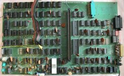
You mean the Sol board? There's only three of them that were ever made, all prototypes, and only one ever worked, and only with a massive number of jumper wires. That board is in the hands of CHM, the second one that appeared in the article probably was kept by PM, and the final is still owned by Lee. Lee sent me pics of that board but they're pics, not scans. I doubt CHM would be willing to take out their original to scan for us. I'd ask Lee but he's been super helpful already and I don't want to be an annoyance.
 
You mean the Sol board? There's only three of them that were ever made, all prototypes, and only one ever worked, and only with a massive number of jumper wires. That board is in the hands of CHM, the second one that appeared in the article probably was kept by PM, and the final is still owned by Lee. Lee sent me pics of that board but they're pics, not scans. I doubt CHM would be willing to take out their original to scan for us. I'd ask Lee but he's been super helpful already and I don't want to be an annoyance.

Hi,

Yes, I'm interested in the working Sol-20 main board. I'm sure if somebody got it made, they could sell them to people so we could build reproduction Sol-20 computers. I've already seen what looks like reproduction "Personality Modules" online for sale.

It's a simple little USB to Parallel ASCII converter so we could use new affordable keyboards: https://www.walmart.com/ip/MageGee-...tch-PC-Gamer-Office-Windows-Laptop-/474258002

Also, it's easy to convert from Composite RCA Video OUT to VGA with a little adapter cable: https://www.monoprice.com/product?p_id=2509


.
 
A photo of the board is perfectly good to make a replica pcb, I did this with photos, from the internet of the pcb for the Votrax Type 'N Talk unit: have a look at the board in this article:


When I finally got an original Votrax pcb, my replica had turned out practically identical. I also hunted down the correct connectors, switch, period correct axial ceramic capacitors, the Xtal and everything else required to make a proper replica of the original board. This sort of thing increases the probability of everything working first time, which it did. The study of it also found that the manufacturers had inadvertently left out a small section of track work, but the original units worked anyway as luck would have it. It requires a lot of attention to detail to make an accurate replica.

Three things help here:

One is that if the camera angle is off perpendicular with the board surface (as often is the case with a flash photo to avoid reflections) there is a function in photo studio that can correct for that and convert it into what would be a square on image.

One other thing, because of the known IC sizes and pin spacing and known some other component geometry, it sets the scale of the whole board.

Also, I have found that most of the pcb's of this era, the designers tended to lay IC's and component holes over a 2.54mm (1/10") grid and place the vias (often but not always) on those or at regular positions in between those. I reconstruct the pcb pads/holes over the grid as a transparency and remove the grid later.

Obviously, a scan is better and saves some time creating a replica, but it is not always available. It also helps to have the schematic at a minimum (or the real original board) to determine the tracks hiding under the IC's, for the Type 'N Talk unit I resolved those from the schematics.
 
Last edited:
A photo of the board is perfectly good to make a replica pcb, I did this with photos, from the internet of the pcb for the Votrax Type 'N Talk unit: have a look at the board in this article:


When I finally got an original Votrax pcb, my replica had turned out practically identical. I also hunted down the correct connectors, switch, period correct axial ceramic capacitors, the Xtal and everything else required to make a proper replica of the original board. This sort of thing increases the probability of everything working first time, which it did. The study of it also found that the manufacturers had inadvertently left out a small section of track work, but the original units worked anyway as luck would have it. It requires a lot of attention to detail to make an accurate replica.

Three things help here:

One is that if the camera angle is off perpendicular with the board surface (as often is the case with a flash photo to avoid reflections) there is a function in photo studio that can correct for that and convert it into what would be a square on image.

One other thing, because of the known IC sizes and pin spacing and known some other component geometry, it sets the scale of the whole board.

Also, I have found that most of the pcb's of this era, the designers tended to lay IC's and component holes over a 2.54mm (1/10") grid and place the vias (often but not always) on those or at regular positions in between those. I reconstruct the pcb pads/holes over the grid as a transparency and remove the grid later.

Obviously, a scan is better and saves some time creating a replica, but it is not always available. It also helps to have the schematic at a minimum (or the real original board) to determine the tracks hiding under the IC's, for the Type 'N Talk unit I resolved those from the schematics.

Hi,

I have one Votrax SC-01 chip and one extra SPO256-AL2 chip. I built two boards for the other two my SPO256-AL2 chips. I still want to build-up a board for the Votrax SC-01 chip some day.
 
So I've made a bit of progress. First, to add to the challenge that the schematic is extremely difficult to follow in several places due to the poor scan quality (especially identifying part ID's and pin numbers), there are definitely some inconsistencies between it and the board layout that I'll need to study a bit more. That said, so far I've only located three obvious board errors. I suspect that the board will need to be built to determine where any 'not so obvious' errors may exist.

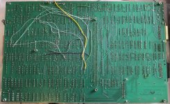
It turns out that most all of the unconnected pads are actually intended for the many bodge wires that connect to the S-100 connector and the I/O ports it seems. I've got a bit more to do, but I've been able to identify/document the target S-100 pins for most of these pads.

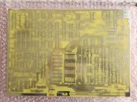
@falter ... in this video, you show pics of the top and bottom of the bare etched board (although they are both inverted). Can you share the original photos? Interestingly, the errors that I found appear to be present in those pics, leading me to believe that the layout scans were used exactly as is to make the board in the picture (which is a good thing). Also, I think I recall that you mentioned that some photos were sent directly to you, in addition to the photos posted on bitsavers. I was hoping to get a somewhat clearer pic of the top of the board to aid in part identification if at all possible. Thx.
 
It turns out that most all of the unconnected pads are actually intended for the many bodge wires that connect to the S-100 connector and the I/O ports it seems. I've got a bit more to do, but I've been able to identify/document the target S-100 pins for most of these pads.

It's good to know that they have a purpose, because looking at all those mysterious hanging chads pads literally had me wondering if the etch patterns for the two sides were from different revisions. It's still pretty horrifying that they went to press with it in that state, though. It's no wonder that they sent out that letter basically begging people not to build that version of the board and wait for the final (as eventually shipped) SOL-PC.
 
It's good to know that they have a purpose, because looking at all those mysterious hanging chads pads literally had me wondering if the etch patterns for the two sides were from different revisions. It's still pretty horrifying that they went to press with it in that state, though. It's no wonder that they sent out that letter basically begging people not to build that version of the board and wait for the final (as eventually shipped) SOL-PC.

I am a bit surprised that they sent the original 'detailed' packet out to anyone, all things considered. Perhaps the packet that was mailed out to the few that sent for it contained more detail than the scans that are provided on the sol20.org web site (although the wording in the Popular Electronics feature didn't list anything more that what are provided with the current scans).

It seems that the design intent was to make the S-100 slot somewhat optional, thus the bodge wire approach. Even the onboard 5204 eproms and 2101 RAM chips aren't usable without additional wiring, presumably to allow the user to use them or something else on the s-100 bus.
 
. Even the onboard 5204 eproms and 2101 RAM chips aren't usable without additional wiring, presumably to allow the user to use them or something else on the s-100 bus.
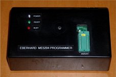
I have mentioned this before on post #81, here is a picture. If you are going to use the MM5204 Eproms to help keep it original, and you don't have the programmer yet, I would recommend Martin Eberhard's ME5204. It is a wonderful machine, super well supported by the manual and the firmware that he designed. He supplies the PCB & the programmed cpu and the BOM. He did a stellar job on it. I used it to program MM5204's for my replica SoL-20 personality modules:


Attachments

  • ME5204.jpg
    ME5204.jpg
    107.4 KB · Views: 13

Hi,

Any chance to see the flip side of the board?

Do you have a good working board now?

We need a new Replication Sol-20 that can use a standard USB keyboard INPUT and have a VGA OUT plus a personality module that hosts a CF card, or SD card, or microSD card to be a "disk drive" on the Replicator Sol-20.


.
 
Hi,

Just today I snagged a real Sol-20 main board and the S-100 extender back plane. Next I need a couple of chips for the main board, then a Personality module or two. I have two keyboard encoder chips and a TRS-80 Model II keyboard I hope to convert to work for the Sol-20.

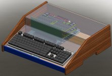
I figure I'll build a cabinet from 5mm plywood and paint it blue, make side panels from Walnut or Oak with a dark stain. I figure for power supply I'll find something like a Mean-Well that has the outputs or maybe just get three Mean-Wells like I did for my Altair 8800c and IMSAI-JAIR computers.

IF anybody has links to sources I would appreciate them.

Yes I know about Sol20.org ...


.
 
What rev. is this board?

The picture that I posted isn't of a SOL-20, it is a replica of an early prototype board that eventually morphed into the SOL-20. It was never really produced, and there are no known operational prototype boards to my knowledge. That board and the SOL-20 board are completely different.
 
Took a break from TVT building and plunged headfirst into the terminal project.

This is going to be oodles harder than any of the others:

1) Very tightly packed, thin traces.
2) Messy artwork.
3) It's double-sided
4) At 9.5x13.5, this is way bigger than any board I've ever made

To simplify things, I'm going to call the artwork I'm using the 'prototype' artwork. From what I now understand, readers of PE could write in for plans to build their own Sol terminal using this artwork. However, there were also drilled and etched boards on offer, and what eventually shipped was *not* using this design. It was using what became the Sol-20 design, with personality modules and all that. In three weeks of searching I have not found a single instance of someone building using the prototype design, and the sol20.org site says it didn't work.

Anyway, with a Mark-8 build and other stuff in the pipeline, it'll take me a long time to get there -- but I figure I'll start working on the artwork. The scan is regrettably messy (or the artwork itself was) and I need to clean it up and make sure we're not having any unwanted shorts. I used Threshold to black and white it.. and for now am using the marquee and fill tools to clean up the clutter one bit at a time. It'll take a long time this way and that sucks.. I'm hoping along the way I find a tool of some sort that'll help.

View attachment 1015405

I haven't quite wrapped my head around how I'll print the toner transfers for it. I'm thinking I will have to break it into segments somehow and print each side on multiple press'n'peel.
Hi,

IF you have the tenacity to do so, creating Gerber files can be a difficult task that leaves you feeling like you accomplished something.

OTOH, IF you want the job done and just get the Gerber files so you can build a board, then tell these guys I sent you: http://www.mhtest.com/scanning.shtml

I have a couple of Processor Technology boards I plan to get scanned into Gerber files when I can afford it.


.
 
Back
Top