• Please review our updated Terms and Rules here

Commodore pet 2001-8 no video from logic board

But it is a very cool circuit. I like the fact we can get inside it.

If one of many failures occurs inside a CRTC chip, it spoils fault finding fun, because you put in a new one and the fault goes away and you are none the wiser what the fault was, almost too easy and not as much fun.

I kind of prefer circuits with lots of TTL IC's rather than LSI chips for this reason. Plus, nearly all the original TTL's are still easy to get, unlike a lot of more modern parts that go obsolete ASAP. I'm glad my PET has this interesting & unusual circuit and not the CRTC chip !

Plus, the more faults that crop up in it as time goes by and we problem solve them, the more familiar we will become with the circuit. You don't get that learning experience, not to the same extent at least, plugging in new LSI chips.
I agree. Usually my approach due to lack of knowledge would be to go around replacing parts until I reach the culprit. This has been alot more time consuming but I have learnt alot and enjoyed it. The flip flops and frequencies confuse me though.
 
Last edited:
I tried both ways. Made no difference to the reading.
OK then, I see now why the upper bits of the counter are jittering and it is not due to the scope trigger. There is a reset to the counter A1, and it is pulsing about 4 times to fast as it is the clock to the sequencer which we know is 4 times to fast.

So A1 and B1 are probably OK. The problem is a signal in the network that drives the gates in the bottom middle of the schematic (page 3). Some signal is probably open/stuck high and not letting the circuit wait to decode the proper count. We will have to follow back from the signals that drive pin 4 and 5 to the D8 NAND gate (don't worry that it is shown as a negative input OR gate. The designer used De Morgan's theorem to show how the gate is functioning i.e., either input pulses Low, the output pulses High).
Just to be 100% I will check A1 and b1 again later today with triggering on manual and auto as I only checked a couple of troublesome pins before. There is a lot of corrosion on some of these ics
 
I had some corrosion on the IC pins of an Apple IIe disk controller. It transpired that some of the pins had actually been 'eaten' through and were not making contact with the IC itself. As a result, these inputs were floating.

I removed the IC's from their IC sockets (all of the devices were in IC sockets - so this was corrosion on the actual IC pins themselves) and ended up leaving various pins behind in the sockets! Interestingly, it was mainly a particular batch of 74LS74 devices that was to blame.

Once the offending ICs were replaced we were in business.

Dave
 
OK then, I see now why the upper bits of the counter are jittering and it is not due to the scope trigger. There is a reset to the counter A1, and it is pulsing about 4 times to fast as it is the clock to the sequencer which we know is 4 times to fast.

So A1 and B1 are probably OK. The problem is a signal in the network that drives the gates in the bottom middle of the schematic (page 3). Some signal is probably open/stuck high and not letting the circuit wait to decode the proper count. We will have to follow back from the signals that drive pin 4 and 5 to the D8 NAND gate (don't worry that it is shown as a negative input OR gate. The designer used De Morgan's theorem to show how the gate is functioning i.e., either input pulses Low, the output pulses High).
This is what I was wondering about on post #350 where I suggested:

The control signal for the J input signal comes via C6 pin 11. Both of C6's inputs and its output need checking on the scope, on channel on the other and the other channel checking the two inputs separately. And one of the inputs to C6 is the result of the decoding performed by E8 , via D8.
 
That was my original plan... I'm not sure which... I would suspect E8 or B1... I'm still inclined to stick with B1... fancy a wager? Either way the OP needs some 74LS20 devices.
 
That was my original plan... I'm not sure which... I would suspect E8 or B1... I'm still inclined to stick with B1... fancy a wager? Either way the OP needs some 74LS20 devices.
I think the B1 wager is good, that is if the A1 counter is not receiving resets altering what would be a regular divide by 8 of the 15.7 kHz clock.

This circuit is interesting because it is the digital analogy of a feedback loop. If something goes wrong, it affects everything inside the loop.
 
IMHO it's really really clever. I wonder who the designer(s) were? It's taken me a long time to get to grips with it.

In the case of the analog loop at least, there is a technique that works to fault find it. In theory the method should also work with a digital loop.

The idea is that you break the loop. At that broken point, where an output is connected to an input, you inject the correct level signal (both AC & DC conditions) into the input. Then you can follow the signal through the circuit to find the fault.

In the digital case it would involve injecting a pulse of the same frequency and duty cycle into the loop. Except that notion is inconvenient, if you are dealing with 8 bits of "feedback" vs one signal line in an analog scenario.

I was thinking, since Commodore did not really provide an adequate description of this creative circuit design, when we figure it out, we should write up a detailed description of it. Maybe they wanted to keep it "proprietary" . Atari did this with their early video games like Pong, they figured by not publishing a circuit description, just the schematic, it might keep most in the dark. Better than paying a fortune to Lawyers in Patent fees and have most others in the world getting around the patents anyway, by making small improvements and claiming a new and better design.

Now similar protection is done by custom firmware embedded in PIC micros, that you cannot read out easily. Again it saves a fortune vs inept patent protection, that most of the world in the far east ignores.
 
This is where Nivag's magic digital fingerprint module would come in...

If the fingerprint of the input signals are as expected, but the fingerprint of the output signal is not - we have a faulty component. Simples...

Dave
 
Breaking the loop....Actually... that's not a bad idea.

Now that A1 has been replaced, and presumably socketed... if you were able to bend out leg 2 of A1 and re-insert it... (i.e. all pins as usual except pin 2 sticking out to the side) and then observe pin 8 of B1...?

I'm assuming it, pin 2 A1, will float high... if not short pin 2 to pin 3 of A1

That would be super interesting... we could look at pins 9, 8 and 11 of A1 and pin 8 of B1.

@RetroGadgetMan are you game to try that?
 
Last edited:
Breaking the loop....Actually... that's not a bad idea.

Now that A1 has been replaced, and presumably socketed... if you were able to bend out leg 2 of A1 and re-insert it... (i.e. all pins as usual except pin 2 sticking out to the side) and then observe pin 8 of B1...?

I'm assuming it, pin 2 A1, will float high... if not short pin 2 to pin 3 of A1

That would be super interesting... we could look at pins 9, 8 and 11 of A1 and pin 8 of B1.

@RetroGadgetMan are you game to try that?
I'm on it.
I socket all replacements.
With pin 2 of A1 out of the socket first observation is noting on the screen which I suspect is normal.
Trigger set to norm
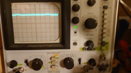
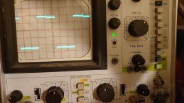
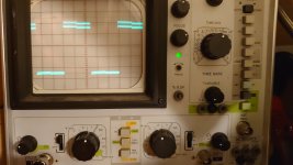
Pic 1 Pin 8 of B1 10us
A1
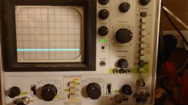
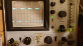
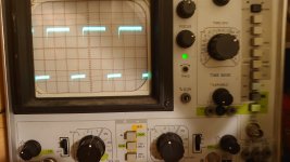
Pic 2 pin 9 5us
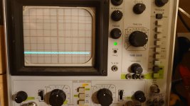
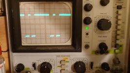
Pic 3 pin 8 5us
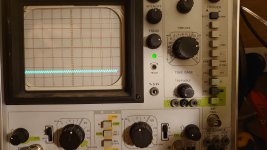
Pic 4 pin 11 5us
 

Attachments

  • DSC_0851.JPG
    DSC_0851.JPG
    780.7 KB · Views: 3
  • DSC_0852.JPG
    DSC_0852.JPG
    863.4 KB · Views: 3
  • DSC_0853.JPG
    DSC_0853.JPG
    832.6 KB · Views: 2
  • DSC_0854.JPG
    DSC_0854.JPG
    955.4 KB · Views: 2
I'm on it.
I socket all replacements.
With pin 2 of A1 out of the socket first observation is noting on the screen which I suspect is normal.
Trigger set to norm
Pic 1 Pin 8 of B1 10us
A1
Pic 2 pin 9 5us
Pic 3 pin 8 5us
Pic 4 pin 11 5us
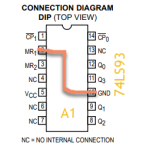
Ah... pin 2 is reset... we need it lo... please add a jumper wire from the dangling pin 2 to pin 10 (solder to the shoulder of pin 10)
 
Though thinking more about this, if A1 is receiving resets at times, which we know it must be from the same pulses that clock the state machine, and we know A1's clock is good, and the divide by 8 comes about due to the counter counting from 000 to 111 binary and then overflowing, ultimately this counter system could only be, on the average, slowed down by resets at a vertical rate, not sped up, because after a reset is would take more clocks starting from 000 to get to 111 again. So the money is still on B1 for now. It is just that those resets are fouling up a good scope acquisition of B1's output.
 
Sure
A1 pin 1 20us
Cool...

So really it should be pretty simple now...

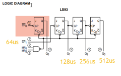
1669052729270.png
Ignore the first gate... We have 64us period pulse going in... should get divide by 2 on pin 9 (that's correct)... divide by 4 on pin 8... and divide by 8 on pin 11...

I'm not really seeing that on pin 8 and pin 11... maybe increase the timebase to make those fit?

On B1 pin 8 we should see a low when display is ON (during horizontal active period) AND count on pins 9, 8, 11 of A1 is HI, HI, HI.... which will be at 1/8th frequency of A1 pin 1.

But... on B1 pin 8 we see something with a period of 250us?? (We are aiming at 512us; i.e. 1/8th of 15.6kHz = 1.953kHz)

My brain is a bit melted by this but I think that is wrong... but not in the way I expected?? I'm still thinking Replace B1
 
Last edited:
Back
Top